
Procedure to Inspect Stencil.
To fulfill technological demands in today’s manufacturing environment, ever-increasing levels of technology necessitate higher product quality, as well as improved inspection and quality control.
Stencil number and details will be pasted on stencil bar as below given image.

Fig 1: Label of stencil
- Check and verify each parameter with received invoice / PO.
- Place the stencil on the bare PCB, align the openings of stencil with pads of PCB. Use fiducial marks for better alignment.
- Check at all points whether all pads were aligned exactly with stencil opening. If ok, we can proceed with next PCB by repeating the same.
- In case of MIS alignment, we have to check whether we aligned with correct PCB or not. If we checked with correct board, we have to check Gerber of particular PCB.

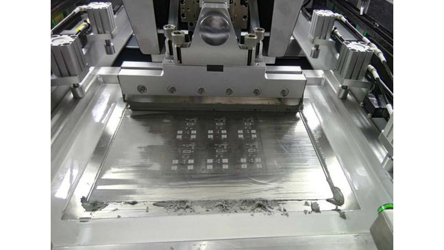
Fig 2: PCB pads misaligned with stencil (Not Ok)

Fig 3: PCB pads exactly aligned with stencil (Ok)
Fig 3 refers a board aligned with stencils.
In Fig 3,
A: Pads of PCB aligned exactly with stencil openings.
B: Pads of PCB misaligned with stencil openings. In such case, we need to check the Gerber which is used to fabricate the stencil with physical board so that we can find reason for misalignment.
While aligning stencil with PCB, if all pads have exactly aligned with stencil opening as fig 3, then stencil is ok.
If any misalignment as ‘B’ in fig 2, stencil is not ok and we should proceed further required steps.
Procedure to apply solder paste on bare PCB by stencil
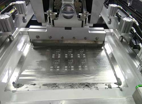
Fig 4: Solder Paste Printing Process
- Place the stencil to the top of the bare PCB.
- Align the bare PCB with stencil opening using fiducial marks.
- Once the stencil is properly aligned on top of the board, solder paste is applied over the openings (making a single pass, using a metal squeegee blade).
- When stencil is separated from the board, solder paste will remain, ready for placement of components.
Typical PCB Stencil Manufacturing capabilities
Manufacturing PCBs can be complex with extensive consumption of resources and time. Stencils help you ensure each component is assembled to perfection on the board after the solder paste has been applied to it. Moreover, stencils ensure your human capital resources and time are optimally expended.
- frameless & framed Stencils
- Micro stencils , mini stencils and full board stencils for solder paste applications as per IPC-7525B standard.
- stencil frame material : Aluminium.
- stencil foil material : stainless steel.
- stencil foil thickness : 4/5/6/8 mil.
- Stencil size offered ; ”*29”, 25”*25”, 23”*23”, 22”*22”, 20”*20”
- Frame width : 40mm
- stepped stencils solution for optimized solder paste release and improved volumetric repeatability for complex component mixes.
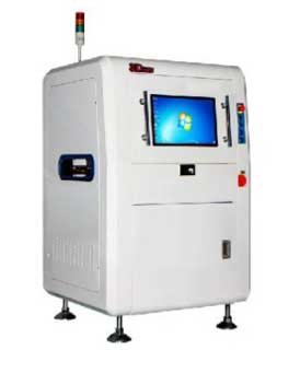
Fig 5: Solder Paste Inspection Machine
EMSxchange Enables you to select a Printed Circuit Board assembly suppliers meeting your Required PCBA Manufacturing Capability, capacity and Certification Criteria from a global PCB Assembly manufacturer base. EMSXchange takes complete responsibility and ownership for your electronic manufacturing process and all its deliverables from contract manufacturing supplier selection to manufacturing to quality inspection to shipment and delivery to your door. EMSxchange Electronic Manufacturing Partners Profile includes:
Argus Sytems (AESPL) – PCBA, Cable Assembly, Box Build.
Cerra Systems inc – PCB Manufacturing.

