
PCB Design for EMI/EMC Compliance
- Electromagnetic Compatibility (EMC) is the capability of electrical and electronic systems, equipment, and devices to operate in their intended electro-magnetic environment within a defined margin of safety, and at design levels of performance, without suffering or causing unacceptable degradation because of electromagnetic interference. (ANSI C64.14-1992)
- Electromagnetic Interference (EMI) is the process where disruptive electromagnetic energy is transmitted from one electronic device to another via radiated or conducted paths.
- Radiated Emissions The component of RF (roughly 10kHz to 100GHz) energy transmitted through a medium, usually free space (air), as an electromagnetic field.
- Conducted Emissions The component of RF energy transmitted as a propagating wave generally through a wire or interconnect cable. LCI (Line conducted interference) refers to RF energy in the power cord.
- Susceptibility is the measure of a device’s ability to be disrupted or damaged by EMI exposure.
- Immunity is the measure of a device’s ability to withstand EMI exposure and still operate at a designated level. Electrostatic Discharge (ESD) A transfer of electric charge between bodies of different electrostatic potential in proximity or through direct contact
- Radiated Immunity The ability to withstand electromagnetic energy which is propagated through free space.
- Conducted Immunity The ability to withstand electromagnetic energy which enters through external cables and connections (power or signal).
- EMI Containment is Keeping RF energy inside of an enclosure by providing a metal shield or plastic housing with RF conductive paint. Similarly, external RF energy can be kept out.
- EMI Suppression is Design techniques that reduce or eliminate RF energy from entering or leaving without using a secondary method like a shield or metal chassis.
PCB Materials and Construction
The most common Base material is a fiberglass resin called FR-4.
| Material | Dielectric constant | CTE ppm/oC | Loss Tangent (δ) |
| FR-4 glass | 4.1-4.8 | +250 | 0.02-0.03 |
| GTEK | 3.5-4.3 | +250 | 0.012 |
| woven glass/ceramic loaded | 3.38 | +40 | 0.0027 |
| PTFE/ceramic (Teflon) | 2.94 | 0 | 0.0012 |
PCB Copper Layers
The conductive layer of a PCB is usually a sheet of copper that has been etched to form the circuit traces. The copper sheet’s nominal thickness is designated by the weight of 1 square foot of copper of the nominal thickness.
Copper Thicknesses
| Weight (oz) | Thickness (in) | Weight (oz) | Thickness (in) |
| 1/8 | 0.00017 | 4 | 0.0056 |
| 1/4 | 0.00035 | 5 | 0.0070 |
| 1/2 | 0.0007 | 6 | 0.0084 |
| 1 | 0.0014 | 7 | 0.0098 |
| 2 | 0.0028 | 10 | 0.0140 |
| 3 | 0.0042 | 14 | 0.0196 |
2-layer Boards
- Route power traces radially from the power supply
- Route power and ground traces parallel to each other
- Signal flow should parallel the ground paths.
- Don’t create current loops by tying different branches together.
Multilayer Boards
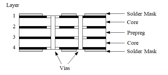
Multilayer boards are formed by etching several double-sided boards and then gluing them together with a material called prepreg. The thickness and material for both the core and the prepreg can be specified and controlled. Vias are holes that are electroplated after drilling and connect the different layers.
Types of Traces
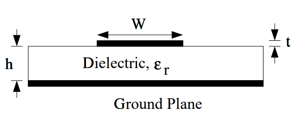
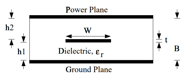
There are two basic types of trace topology: Microstrip and Stripline.
Microstrip
Faster signals are possible due to lower capacitive coupling, but greater radiated RF
Stripline
Greatly reduced RF emissions, but slower signals
- The coupling path is frequency-dependent
- High frequencies are radiatedLow frequencies are conducted
- The boundary is typically about 30 MHz
- There are 5 aspects to EMC when finding the problem
- Frequency – Where in the spectrum is the problem observed?
- Amplitude – How strong is the energy source?
- Time – Is it continuous or intermittent with operation?
- Impedance – What is the Z of the source and receiver?
- Dimensions – What are the physical dimensions of the device that will allow emissions? (RF currents will leave through openings which are fractions of a wavelength!)
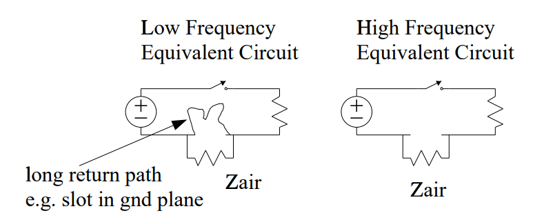
How PCB’s Radiate RF Energy
- Digital signals with fast rise/fall times contain very high frequency components even for low clock frequencies! Fmax =1
- The RF currents from the switching choose the low-impedance path
- The Z0 of air is about 377Ω.
- Discontinuities in the RF return path ZRF> 377Ω
- RF current leaves the board in Favor of the air = EMI
Radiated Emissions
EMI Suppression – Image Planes
An image plane is a layer of copper (either a voltage or a ground plane) which physically adjacent to the signal routing plane. The image plane provides a low impedance path for the RF currents and reduces the EMI emissions since the RF currents use the plane instead of the air.
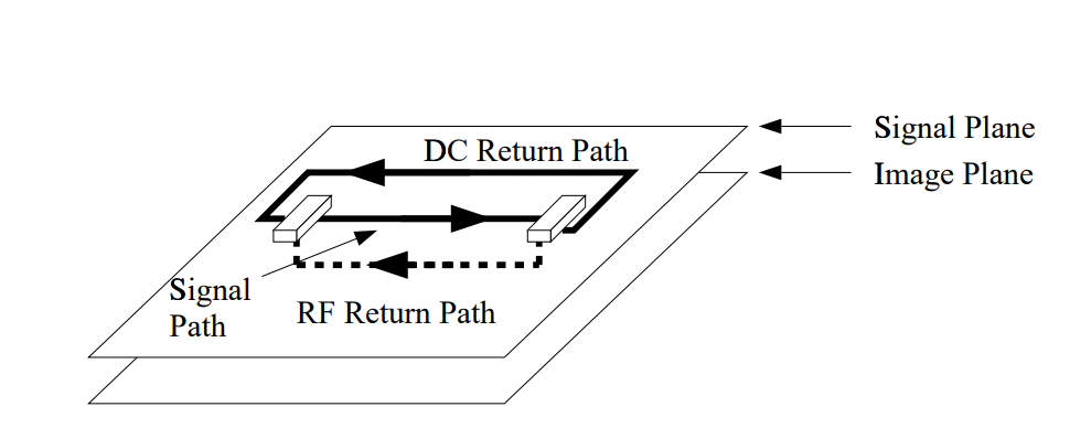
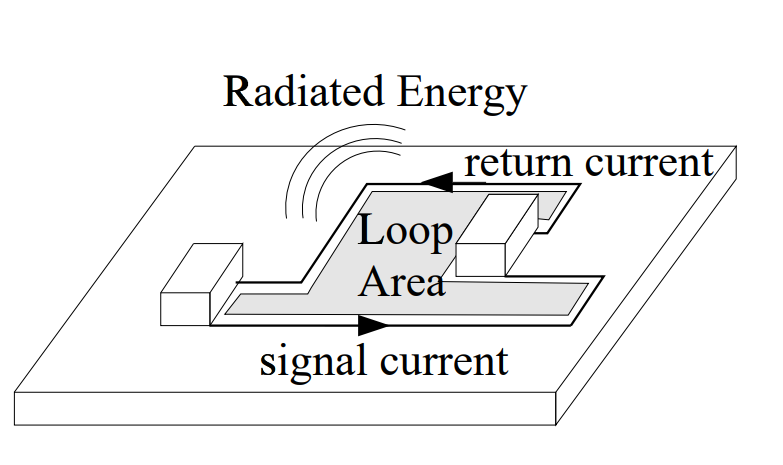
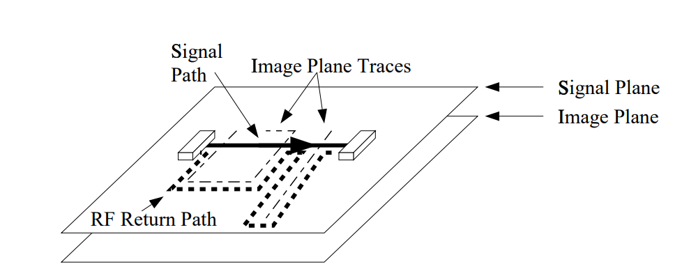
Image Plane Violations
Routing traces in the image plane will create slots in the RF return path and create a large loop area and potential EMI.
EMI Suppression – The 20-H Rule
- RF currents fringing between the power and ground planes at the edge of the board can result in RF emissions.
- Reducing the size of the power plane concerning the ground plane will reduce these emissions.
- This increases the intrinsic self-resonant frequency of the PCB.
- The ground plane should exceed the power plane by 20•H where H is the total thickness between the power and ground planes
- 20-H provides for approximately a 70% reduction of the fringing flux and changing to 100-H will provide about a 98% reduction.
The 20-H Rule in Action
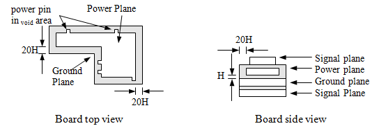
If a power pin needs to be located near the edge of the board, then it is ok for the plane to extend into the 20-H void to surround the pin.
EMI Suppression – System-Level Grounding
There are three main system grounding methods
- Single-Point Grounding
- Either Series or Parallel
- Best for frequencies below 1 MHz
- Has the largest amount of ground loop currents
- Multi-point Grounding
- Preferred for frequencies above 1 MHz.
- Minimizes loop currents and ground impedance of planes.
- Lead Lengths must be kept extremely short
- Provides for maximum EMI suppression at the PCB level
- Hybrid
- A mixture of both Single-Point and Multi-Point Grounding in the same system.
- Ground loops cause RF energy to be radiated when high inductance returns are provided.
- Note: Do not count on mounting screws to provide low inductance connections They are highly inductive and can act as helical antennae at high frequencies (100 MHz-1 GHz)!! (Use conductive gaskets in addition to the screws.)
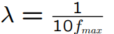
- In a Multi-point ground system, the distance between the screws should not exceed λ/20 of the highest edge rate on the PCB.
EMI Suppression – Partitioning
Partitioning consists of breaking a board up into functional areas concerning the bandwidth of the functional block. Grounding connections are made around the perimeter of each functional block using spring fingers, screws, gaskets, etc, provided that the method has a sufficiently low inductance between the ground plane and the chassis ground.
Signal Integrity – Ringing and Reflection
Transmission line properties which occur between the source and load. Possible causes:
- Changes in trace width
- Improperly matched termination networks
- Lack of terminations
- T-stubs, branched or bifurcated traces
- Varying loads and logic families
- Large power plane discontinuities
- Connector transitions
- Changes in trace impedance
Signal Distortion
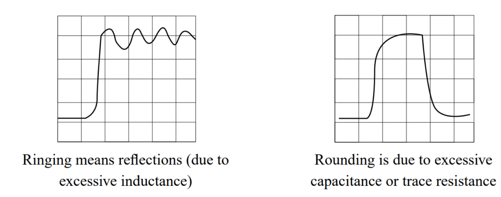
- Ringing is minimized by proper terminations (e.g. series R)
- Rounding means the net is overdamped. Don’t forget about the shunt capacitance of the trace as well as the load capacitance.
Signal Integrity – Crosstalk (aka Board-level EMI)
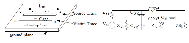
- Crosstalk requires a 3-wire circuit!
- Terminating resistors with a common pin susceptible!
Preventing Cross-Talk
First, note the following observations:
- Decreasing the trace separation increases the mutual capacitance of Cm and the cross-talk.
- With parallel traces, longer parallel lengths increase the mutual inductance Lm and the cross-talk.
- Decreasing the rise time of the signal increases the cross-talk.
Some Solutions are:
- Group and locate logic devices according to functionality.
- Minimize routed distance between components
- Minimize parallel routed trace lengths
- Locate components away from I/O interconnects and other areas susceptible to data corruption.
- Provide proper terminations on impedance-controlled traces or routed traces rich in harmonic energy
- Avoid routing traces parallel to each other. Provide sufficient separation between traces to minimize inductive coupling (The 3 W Rule) or use guard traces.
- Route adjacent signal layers orthogonal to reduce capacitive coupling between the layers.
- Reduce signal-to-ground reference distance separation
- Reduce trace impedance and/or signal drive level
- Isolate signal layers which must be routed in the same axis with a solid planar structure.
The 3-W Rule
This rule for trace separation will reduce the crosstalk flux by approximately 70%. (For a 98% reduction, change the 3 to 10.)
The distance of separation between traces must be three times the width of the traces, measured centrelines to centreline.
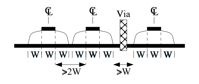
Note that the traces near the edge of the plane need to be > 1W from the edge.
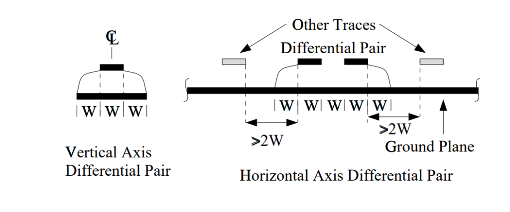
For Differential Pair Traces
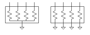
Guard/Shunt Traces
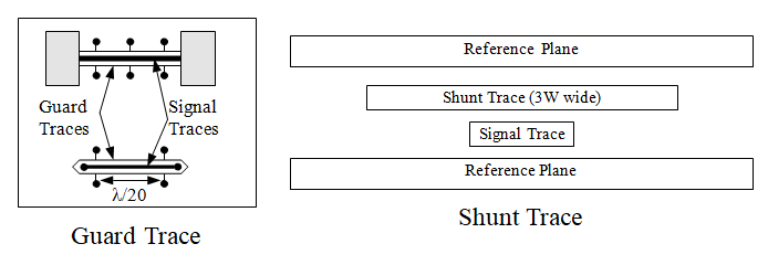
- Guard traces surround the high-threat traces (clocks, periodic signals, differential pairs, etc.) and are connected to the ground plane. They are very useful in 2-layer boards.
- The guard trace should be the smallest, tolerable manufacturable spacing from the signal. The guard trace is connected to the ground.
- If a ground plane is available, make ground connections no farther than λ/20¶ apart.
- Shunt traces are traces located immediately above a high-threat trace and follow the trace along the entire route. They are best used in multi-layer (6 or more) boards.
Guard & Shunt Trace Examples
Power and Ground Bounce
- Ground bounce is caused by the simultaneous switching of drivers in an IC package and may cause functionality as well as EMI concerns. Ground bounce presents a situation where the ground reference system is not at a constant 0 V reference value.
- Be sure to provide a separate ground connection for each ground pin directly to the ground plane. Connecting two ground terminals together with a trace to a single via defeats the purpose of having independent ground leads on the device package.
- Choose component packaging carefully: use devices with a ground reference in the centre of the device to reduce the Lgnd (4nH vs 15nH). Surface mount devices are preferred over through-hole packages for this reason.
Types of capacitor usage
There are three primary uses for capacitors:
- Bulk capacitor Used to maintain constant DC voltage and currents when all signal pins switch. Also prevents power drop out due to dI/dt current surges from the components.
- Bypassing Removes unwanted common-mode RF noise from components or cables by placing an AC-short to ground. This keeps the unwanted energy from entering a protected area as well as limiting the bandwidth. Bypassing is also used to divert RF energy from one area to another.
- Decoupling Removes RF energy injected into the power planes from high frequency components consuming power at the device’s switching speed. They also provide a small amount of energy to function as localized bulk capacitors.
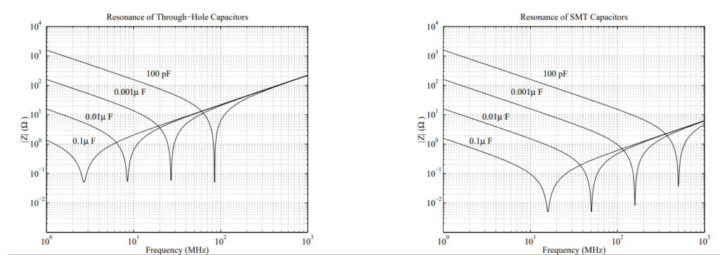
Resonance Effects
Remember, the capacitors really have an ESL and ESR.
- Through-hole: ESL≈35nH and ESR≈50mΩ
- Surface Mount: ESL≈1nH and ESR≈5mΩ
Parallel Capacitors
Remember that the power planes form a capacitor.
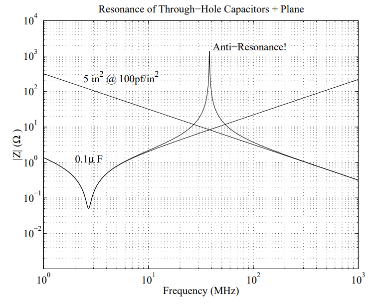
Tips on Paralleling Capacitors
- Parallel capacitors of the same value will increase the net capacitance and reduce the ESL and ESR. The reduction of the ESL and ESR is the most important property. Improvements of 6dB have been observed (replacing one capacitor with multiple smaller ones).
- Be careful to remember that the values will be different and anti-resonance will occur.
- Choose values such that the anti-resonance will not occur at a harmonic of a generated signal (either a switching or transition frequency).
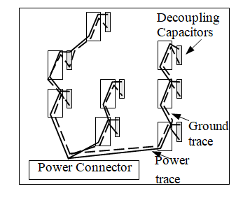
Capacitor Placement
Key idea is to reduce path inductance
- Capacitor placement location is key.
- the location of the components is limited by mechanical constraints.
- SMT parts can be closer than THT parts.
- trace inductance will be 3-10x larger than plane inductance.
- each via adds 1-3 nH of inductance.
Trace Routing
- Keep signal traces away from high-frequency devices, e.g. clocks.
- Do not use auto routers since they typically choose the worst possible layout for EMI/EMC concerns…
- Remember the 3-W rule
- Remember the 20-H rule
- Use isolation (moats) in conjunction with the partitioning
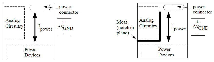
Isolation/Moating
Intentionally introducing breaks in the power and/or ground planes.
WHY???
Consider the following:
Moat Violations
Moat violations will virtually always generate lots of EMI, even if the violating trace is “quiet.”
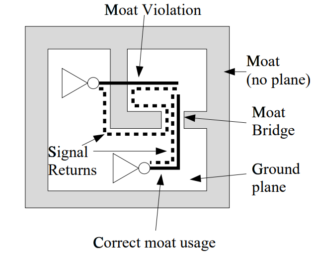
Bridging Moats
- Make the bridge wide enough for just the required traces (observing 3W)
- Use a ferrite to provide filtering in the power trace, but do not put one in the ground traces.
- If a violation must occur, place a bypass capacitor across the moat as close to the violation as possible. Capacitor is connected ground to ground.
- choose for proper filtering bandwidth (RF return current)
- Peak surge voltage capability for ESD protection
ESD Protection
- Provide good shielding with the chassis and connectors.
- Provide good grounding connections; wire braid with a 5:1 width: height aspect ratio is good for example Solder wick works nicely for this purpose.
- Avoid pigtail wiring harnesses. They make good RF antennae and will radiate.
- Filling unused signal planes with a ground fill helps prevent ESD, not EMI.
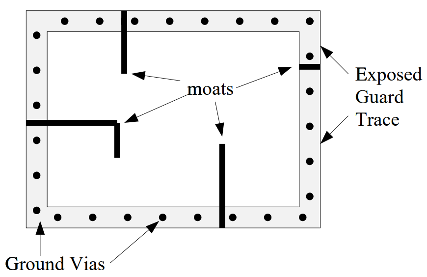
- Guard Bands
Guard Bands
- Different from guard, shunt, or ground traces
- Prevents ESD damage from handling of PCB
- A NON-continuous trace around the edge of the PCB on both the top and bottom layers (introduce some moats to prevent ground loops!).
- Should not be covered with the solder mask and should frequently be connected to the ground reference with vias.
A Guard Band
EMSxchange Enables you to select a Printed Circuit Board, PCB Assembly, cable & wire harness assembly, and box-build suppliers meeting your Required Electronic Manufacturing Capability, capacity, and Certification Criteria from a global Electronic contact manufacturer base.
EMSxchange takes complete responsibility and ownership for your electronic manufacturing process and all its deliverables from contract manufacturing supplier selection to manufacturing to quality inspection to shipment and delivery to your door.
EMSxchange Electronic Manufacturing Partners Profile includes:
Argus Systems (AESPL) – PCB, PCBA, Cable Assembly, Box Build, Testing.
