
What Is PCB Layer Stackup?
Stackup, as the name implies, refers to the collection of copper and insulator layers that make up a PCB before the final design is finalized. Because there is a demand for condensed electronic products, PCB layer stack up is critical in the electronics industry. Designers recognize the necessity for PCBs with numerous layers and a 3d outlook on the design in order for electrical devices to have that condensed design. The various layers aid in improving the board’s ability to distribute energy, enabling high-speed transmissions, eliminating electromagnetic interference, and limiting cross-interference.
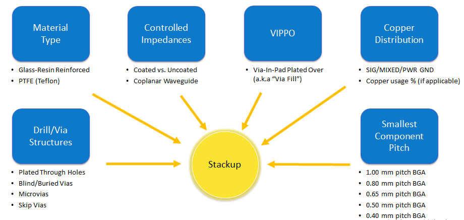
Basic Information Requested to Generate a Stack-up:
- Part number or part name for filing/tracking purposes.
- Board overall thickness, nominal target, and tolerance (+/- 10% tolerance assumed).
- Material type.
- Total layer count.
- Layer type of each (signal, PWR/GND, mixed), and %copper retained on each layer if known.
- Cu thickness/weight required for each layer.
- Any blind/buried via structures, including drill/pad diameter requirements if known.
- Specific controlled impedance requirements by layer (include target trace widths/spacing or constraints if any (i.e. rout differential pairs between specific component pad pitch, etc…).
- Build class (IPC-6012 class 2 or 3).
- Any non-standard requirements (i.e. VIPPO, buried capacitance (BC), etc.).
Key Influences to Stack-up Creation
PCB Stack-up Structure
All design components are constructed upon the foundation of the PCB stack-up. As a result, a badly designed PCB stack-up with wrongly selected materials can have a negative impact on signal transmission, power delivery, manufacturability, and reliability of the circuit assembly.
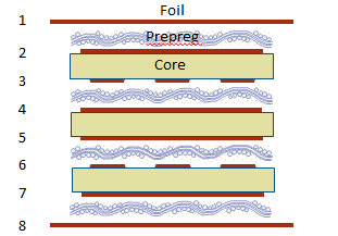
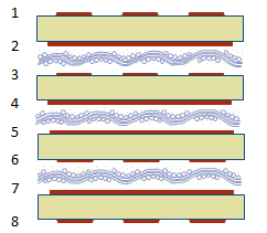
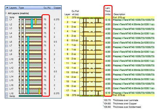
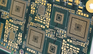
Multiple alternating layers of core, prepreg, and copper foil components are heat-pressed and cemented together to form a conventional PCB stack-up.
A thin electrical insulator (dielectric) with copper-clad foils glued to both sides is used as the core material (a cured fiberglass-weave material with epoxy resin). As a result, the dielectric functions as a barrier between the copper foils. The signal, power, and ground planes (layers) in the PCB are formed by the internal copper. Prepreg connects the main layers and acts as a barrier between them.
The layer arrangement of core and prepreg layers is laminated together with a top and bottom copper layer during the PCB manufacturing process. Heat and pressure are used to bond all of the different (PCB stacks) layers together.
The total number of layers required (layer count)
The following are the most important things to consider when deciding the number of layers required:
- power/ground/signal layer requirements
- board complexity
- component density
- component package types
Channel routing will very certainly need to be accommodated using blind vias in addition to layer configurations for high channel count / high channel density devices to get the optimum signal integrity of the channel.
Layer arrangement
To preserve signal performance and durability, the power plane is frequently positioned directly next to a ground layer in the layer stack-up. In order to reduce the overall number of layers, the power plane is shared as much as possible.
It is recommended that the spacing between adjacent signal layers be increased. When considerable separations are present, however, this can have an impact on the overall thickness of the PCB.
The routing layer for high-speed traces should be planned during stack-up design when high-speed signals are routed on microstrips with a minimum thickness.
Layer material
For tight coupling, place signal layers near internal power layers.
From the top and bottom layers inward, make the stack symmetric.
Material selection
Many Variations of PCB materials exist for specific emphasis on:
- Electrical Performance Characteristics (High Data Rates/Frequencies)
- –Low Loss Df/Dk
- Mechanical Performance Characteristics (High Operating Temp)
- –High Td/Lower CTE
- Thermal Management Attributes (High Wattage/Thermal Output)
- Cost Considerations (High Volume/Consumer Electronics)
- Compatibility with Manufacturing
Often selected with combinations of the above in mind.
Stack-up Constructions
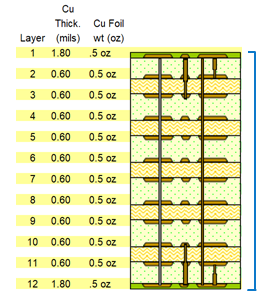
1x Lamination
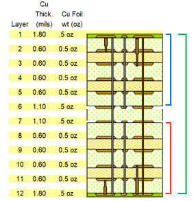
3x Lamination
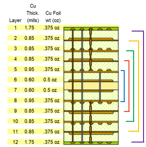
5x Lamination
PCB Stack-up Rules
- The use of ground plane boards is the first rule. They are the best to utilize since they allow signal routing in a stripline configuration. Furthermore, it aids in the reduction of ground noise. Because of the lower ground impedance, the ground noise is greatly reduced.
- High-speed signals must be routed through intermediary layers that sit between the different levels. Ground planes act as a shield, containing the radiation emitted by the tracks as they travel at high speeds.
- It’s also crucial to make sure that the signal layers are close to each other, even if they’re in different planes.
- A signal layer must be in close proximity to a plane.
- The mass and power planes should be meticulously connected.
- Ascertain if the arrangements are symmetrical.
- You should attempt to improve EMI performance as well as noise reduction.
- It is also critical to take into account the thickness of each signal layer.
- It’s also crucial to think about the qualities of the materials you’ll be using. Take note of the materials’ thermal, electrical, and mechanical properties.
- When creating the stack up, you should also think about the applications you’ll be using.
The importance of good PCB design cannot be overstated. It is critical for you to have a high-quality product and end result. As you may be aware, today’s circuits operate at exceedingly high rates, necessitating the greatest possible PCB design. The requirement for appropriate PCB design has elevated the process to the status of art. This is due to the fact that you can either create a good or bad design. The truth is that an electronic product’s performance can be harmed or affected by a PCB with a poor design. It is quite important to ensure that a printed circuit board is well-designed.
Foil vs. Core Construction
Foil Construction
Core Construction
Trade-Offs:
- Foil construction is preferred for manufacturing due to better registration potentials.
- Core construction is preferable for electrical performance. However, manufacturing impacts include:
- Higher risk of misregistration due to core shifting during lamination.
- Higher cost due to more cores needed.
- Core construction may be required based on certain materials (i.e. PTFE).
Copper Thickness
- Internal layers are typically not plated so their copper thicknesses are fixed.
- 0.5 oz., 1.0 oz., 2.0 oz., etc.
- External or “plated” layers start with a thinner copper thickness and get plated up simultaneously with drilled holes.
- 0.375 oz. + plating
- 0.5 oz. + plating
- Pressed thickness decreases with increasing copper thickness, due to the need to fill larger gaps between copper features. Therefore, more plies of prepregs are usually necessary on heavier copper builds to increase the amount of resin available to prevent resin voids/starvation.
Impedance Table Interpretation
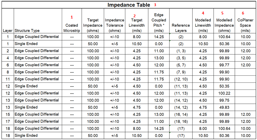
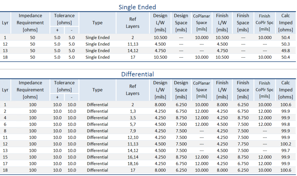
| Column Attributes | Definition |
| Coated vs. Uncoated Microstrip | Modeled or Finish Line Width |
| Target or Design Line Width | The line width that is designed into the customer data as received. |
| Edge Couple Pitch | Center-to-Center distance between differential pairs. |
| Modeled or Finish Line Width | The line width that our simulator suggest that will better meet the target impedance. This is also the line width our CAM operators will adjust to on the tooled data. |
| Modelled or Calculated Impedance | The impedance result based on the modelled or finish line width. |
| Coplanar Space | The spacing between the trace (microstrip or stripline) to adjacent ground plane on the same layer. |
| Design or Finish space | Differential space that is measured from the edge of Trace-to-Trace. |
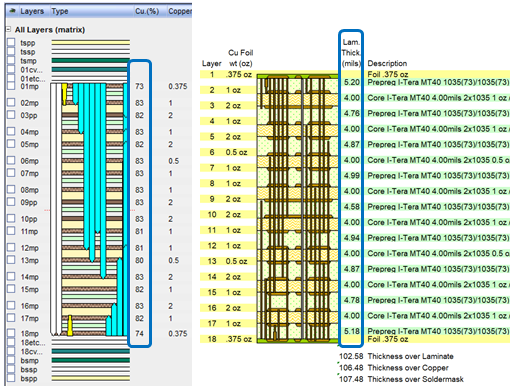
Copper Usage/Retention – Stack-up Perspective
Preliminary Stack-up
*Before Final Data is available*
Default Copper Usage assumes 25% SIG, 50% MIX, 75% PWR/GND

Production Stack-up
*Final Data is tooled and Stack-up is synced with data*
Copper Usage/Retention – Data Perspective

Preliminary Stack-up
*Before Final Data is available*
Default Copper Usage assumes 25% SIG, 50% MIX, 75% PWR/GND
Copper Usage/Retention – Data Perspective
Based on Part Number: 09-066795 Rev A
Production Stackup
*Final Data is tooled and Stackup is synced with data*
EMSxchange Enables you to select a Printed Circuit Board, PCB Assembly, cable & wire harness assembly, and box-build suppliers meeting your Required Electronic Manufacturing Capability, capacity, and Certification Criteria from a global Electronic contact manufacturer base.
EMSxchange takes complete responsibility and ownership for your electronic manufacturing process and all its deliverables from contract manufacturing supplier selection to manufacturing to quality inspection to shipment and delivery to your door.
EMSxchange Electronic Manufacturing Partners Profile includes:
Argus Systems (AESPL) – PCB, PCBA, Cable Assembly, Box Build, Testing.
