
Pattern plating

Pattern plating is a DC electroplating process.
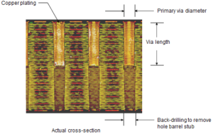
The drilled holes, which are made conducting in the PTH process, are built up to 25 microns, to act as good conductors.
In this process, the copper area exposed during photo printing also gets plated. Hence, the process is called “pattern plating”.
PCB Solder Plate

At the end of the pattern plating, the panels (ckt pattern) are plated with tin metal. This platted tin act as etch resist, to protect plated copper while removing unwanted copper (copper below DFPR) in the subsequent process (alkaline etching)
Etching
Alkaline etching

The resist which was acting as plate resist is stripped (similar to inner layer stripping), exposing the unwanted copper.
The unwanted copper is etched to obtain the required circuit pattern
Tin stripping

After etching, the tin coat (which was acting as etch resistant during etching) is stripped off.
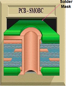
Solder Mask
Solder mask is “a coating material used to mask or protect selected areas of a printed wiring board from the action of an etchant, solder or plating”
Functions of the Solder Resist
- Reduce solder bridging and electrical shorts during assembly
- Protect PWB circuitry from handling damage.
- Provide an environmental barrier
- Fill space between conductor lines and pads with the material of known dielectric characteristics
Hot Air Solder Levelling
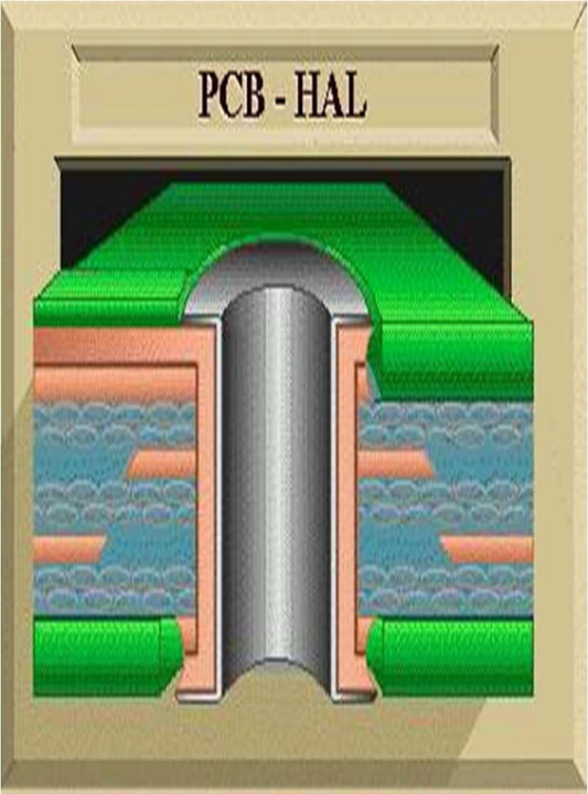
In this process solder (an alloy with 60% tin and 40% lead, or 99% tin–lead-free solder) is applied in the areas where components are mounted, I.e. where connectivity for the electrical components is required.
Solder protects the copper from oxidation and gives better solderability at the time of assembling the boards with components.
Gold Plating
Electro less Nickel gold
- This is an alternative process to HASL
- For surfaces such as contacts or tips that normally receive heavy wear, the use of nickel under gold will greatly increase the wear resistance
Electro Gold plating
- Gold is an excellent resistance for etching. Along with this gold has good electrical conductivity, tarnish resistance, and solderability after storage.
- Gold can produce contact surfaces with low electrical resistance.
- In spite of its continued advantages, the high cost of gold has restricted its major application to edge connectors (tips) and selected areas
Legend
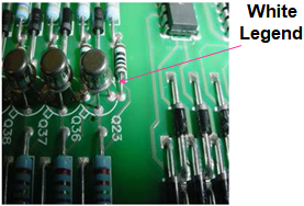
In Legend the identification symbols are screen printed on the board to aid the assembly operation
Carbon Printing
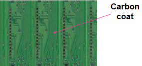
- Carbon coating is a surface finish process an alternative to HASL or ENIG.
- Carbon has the special property of having a very high mechanical resistance and a low electrical resistance.
- The specials property of carbon finds use in Keypads such as Phones, ATM machines, keyboards, etc
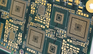
Fabrication
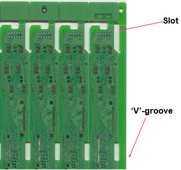
- Fabrication describes many mechanical operations that bring the PCB to its final dimensions, create a specified slot, grooves bevels, or chamfers
- Milling the PCB to its final dimension and slot creation is done in the routing
- In ‘Scoring’, ‘V’ grooves are machined on opposite sides of the– panel to a sufficient depth to allow the user to break apart boards from the panel after assembly.
Bare Board Testing (BBT)
- Finished PCB without any components mounted is called a Bare Board
- Bare board testing is done to check the electrical integrity of the PCB.
- In BBT the boards are checked for opens, shorts, voids, and isolation
- Jigs are used to test the boards. Jigs are test fixtures that are usually constructed by drilling a piece of non-conductive material with the same pattern as the drilled holes, along with the pad (SMT) pattern. Spring-loaded metal pins are inserted in the drilled holes of the test- fixture to make contact with the corresponding- points on the PCB to be tested. The opposite ends of the metal pins are connected by wire to the test equipment.
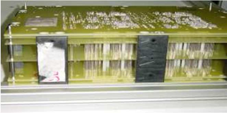
BBT Jig
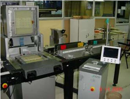
BBT machine
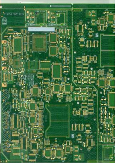
Final Inspection
- The final step in the manufacturing process is a visual inspection of the finished PCB.
- In the final inspection, PCBs are checked for correct mechanical dimensions and are visually examined for overall appearance and other cosmetic parameters
AQL (Acceptance Quality Level)
The AQL is a visual inspection of the finished PCB after the Final Inspection on a sampling basis.
In AQL PCBs are checked for correct mechanical dimensions and are visually examined for overall appearance and other cosmetic parameters.
Packing
The final step in the manufacturing process is packing, after the AQL the boards are packed as per the specification.
EMSxchange Enables you to select a Printed Circuit Board, PCB Assembly, cable & wire harness assembly, and box-build suppliers meeting your Required Electronic Manufacturing Capability, capacity, and Certification Criteria from a global Electronic contact manufacturer base.
EMSxchange takes complete responsibility and ownership for your electronic manufacturing process and all its deliverables from contract manufacturing supplier selection to manufacturing to quality inspection to shipment and delivery to your door.
EMSxchange Electronic Manufacturing Partners Profile includes:
Argus Systems (AESPL) – PCB, PCBA, Cable Assembly, Box Build, Testing.