
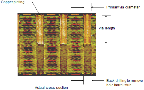
Back drilling Technology Overview
Back drilling, or controlled depth counter boring, is a process where plating is removed from the unused portion of the via. Multi-layer Printed Circuit Boards (PCBs) are processed in a standard manner, adding a secondary drilling operation after plating using PCB CNC drilling equipment with controlled depth capabilities. CNC drill files created from customer data allow this process to be automated and repeatable.
The energy that is transitioning through the plated hole uses the hole as a transmission line element whose parameters are defined by the physical dimensions of the structure (pad size, anti-pad size, dielectric), It then reaches an impedance-matched stripline layer. Some of the energy is transmitted into this layer and some continue to travel down the remaining via (reflects back to the driver).
Any portion of the plated through the hole below the exiting stripline layer can be looked at as an open transmission element referred to as a stub.
Back drilling, or counter boring, the via is an alternative technique to minimize the stub. Back drilling is simply drilling out the unused portion of a via to a controlled depth on the same type of mechanical drill equipment used to initially produce the PCB.

An important parameter is the secondary drill diameter. This drill diameter must be greater in diameter than the primary drill to allow the removal of all the electrodeposited plated metal, typically copper with an additional surface finish. Minimization of this diameter is important to avoid the reduction of routing channels which compromise hole-to-trace spacing in the pin fields.
The current recommendation is 0.008” – 0.006” over the original drill diameter depending upon depth. Drill-to-copper ranges from 0.008” – 0.006”.
- Back drilling is a trade-off between manufacturing cost and electrical performance.
- Contributors to back drill depth variations are mechanical depth and layer position.
- An optimized process achieves a 3 sigma overall variation of +/- 0.005” to nominal target depth.
- At least a 0.010” target nominal depth before the last layer is connected is recommended.
Back-drilling To Optimize Via Transition

Frequency Sweep DC to 15 GHz

Depth = 0
Depth = 0.005” (surface pad removed) Depth = 0.015”
Depth = 0.030”
Depth = 0.045”
Depth = 0.060
PCB design rules for single lamination constructions
Primary drill to copper: 0.012” Standard, 0.009” Advanced
Back-drill diameter: Primary drill + 0.008” standard, 0.006” Advanced
Back-drill to copper: 0.008” Standard, 0.006” Advanced


Drill 0.010” (250 µm) over the original drill diameter
Z tolerance = + /- 0.005” (150 µm)
Drill location tolerance = +/- 0.002” (50 µm)
PCB thickness = +/- 10%
Back Drilling Goal is to minimize Stub Length. Variation in Stub Length depends upon:
- Variation in Mechanical Drill depth
- Variation in PCB overall thickness
- Variation in Layer Depth

Stub Length of 0.012” (300 µm)
Back Drilling Offering
- Low-Cost option
- Variable depths
- From one side or both sides
- Reduces routing real estate
EMSxchange Enables you to select a Printed Circuit Board, PCB Assembly, cable & wire harness assembly, and box-build suppliers meeting your Required Electronic Manufacturing Capability, capacity, and Certification Criteria from a global Electronic contact manufacturer base.
EMSxchange takes complete responsibility and ownership for your electronic manufacturing process and all its deliverables from contract manufacturing supplier selection to manufacturing to quality inspection to shipment and delivery to your door.
EMSxchange Electronic Manufacturing Partners Profile includes:
Argus Systems (AESPL) – PCB, PCBA, Cable Assembly, Box Build, Testing.