
HDI PCB Manufacturing Process
The following is an outline of the manufacturing process to produce an 8-layer IPC Type II HDI printed circuit
IPC Classifications For Rigid PCBs
The Institute for Interconnecting and Packaging Electronic Circuits (IPC) IPC 6011/6012 Circuit Classifications (Rigid Circuits)
- Type 1
- Single-Sided
- Type 2
- Double-Sided
- Type 3
- Multilayer without blind or buried vias
- Type 4
- Multilayer with blind and/or buried vias
- Type 5
- Metal core Multilayer without blind or buried vias
- Type 6
- Metal core Multilayer with blind and/or buried vias
IPC Classifications For HDI PCBs
The Institute for Interconnecting and Packaging Electronic Circuits (IPC) IPC 2226A Classification of HDI Types
- Type 1
- 1 [C] 0 or 1 [C] 1 – with through vias connecting the outer layers
- Type 2
- 1 [C] 0 or 1 [C] 1 – with buried vias in the core and may have through vias connecting the outer layers
- Type 3
- ≥ 2 [C] ≥ 0 – may have buried vias in the core and may have through vias connecting the outer layers
- Type 4
- ≥ 1 [P] ≥ 0 – where P is a passive substrate with no electrical connection
- Type 5
- Coreless constructions using layer pairs
- Type 6
- Alternate constructions
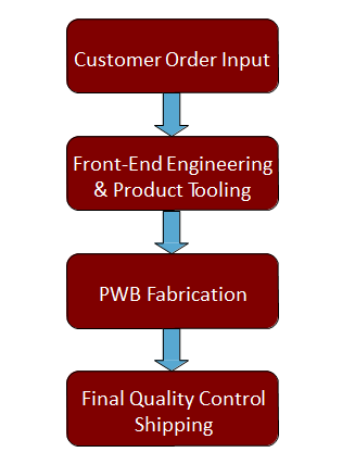
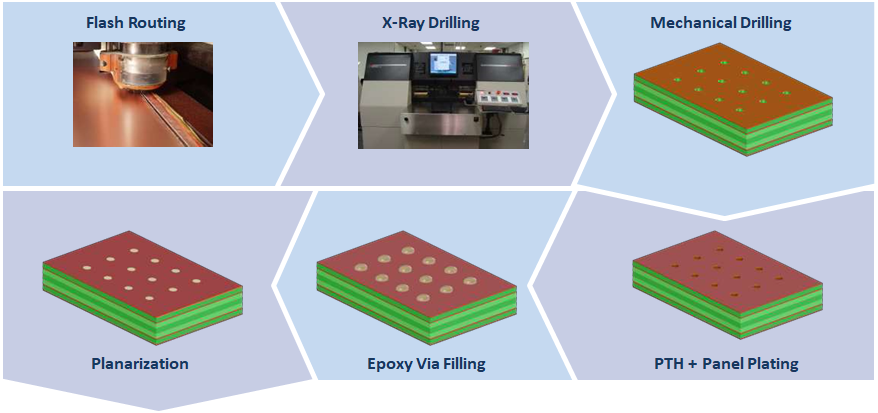
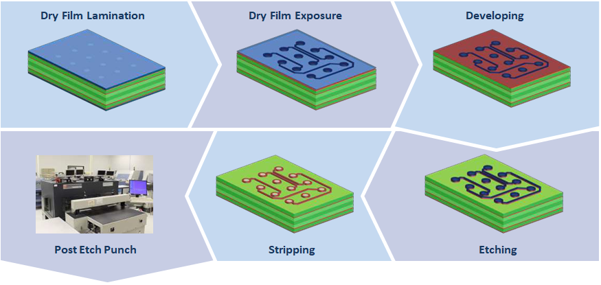
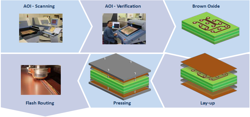
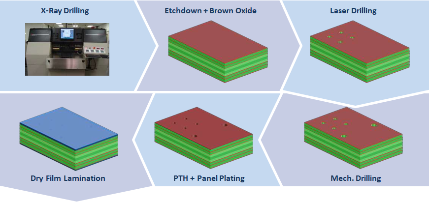
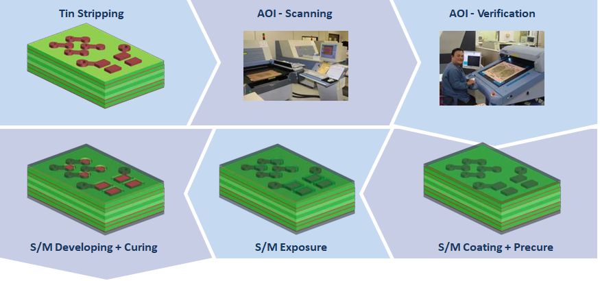
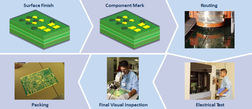
Basic Process Flow
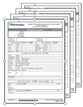
Manufacturing Instructions (MI)
- Analyze data (Gerber file, drawings, netlist, etc.)
- Raise issues in TQ and confirm with the customer
- Create Manufacturing Instructions and CAM
Instructions
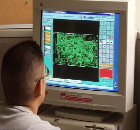
CAD/CAM
- Panelize Customer data (step and repeat data on a panel)
- Add test / TDR coupons & tooling locations
- Create Drill files, Layer files, Rout files, Electrical test data, etc.
- CAD Reference files (each layer) for AOI
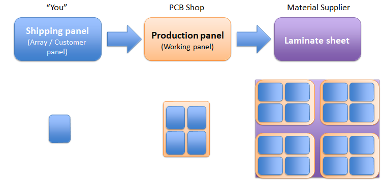
Panelization
1+6+1 HDI
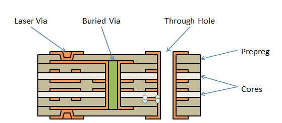
Start production with cores (inner layers) first
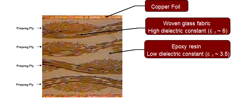
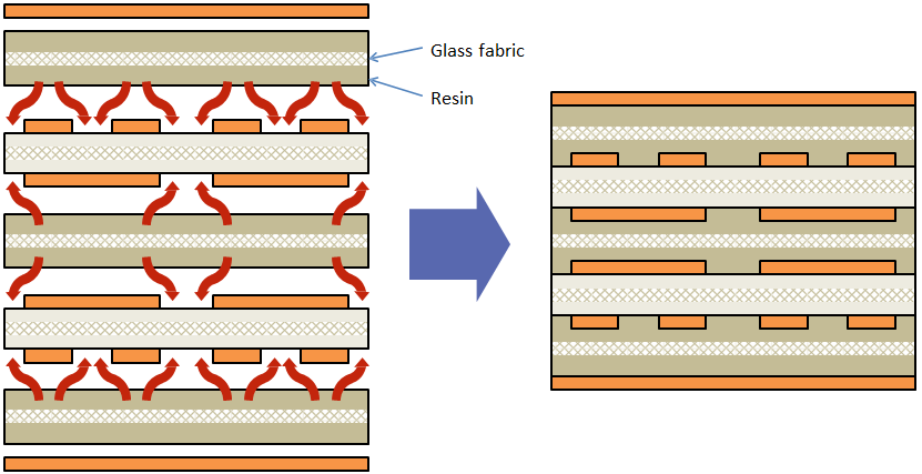
Epoxy-Glass Laminate Construction
- Dielectric constant of the composite laminate is a function of the resin/glass ratio
- Composite laminates can have many different resin/glass constructions
- Heavy glass fabric can have fiber bundles that are Larger than the actual copper trace
Inner Layer
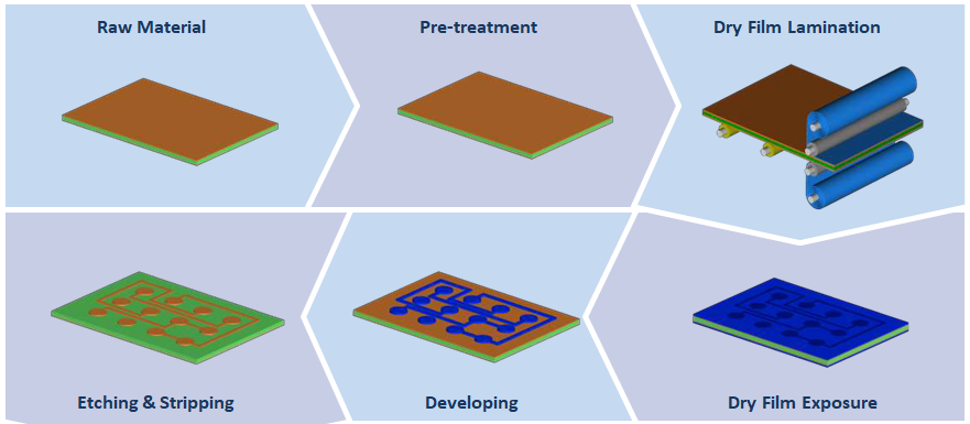
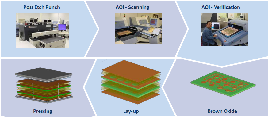
Pressing (Lamination)
Inner Layer (Sub-Assembly)
Inner Layer (Sub-Assembly) -> Outer Layer
Outer Layer

EMSxchange Enables you to select a Printed Circuit Board, PCB Assembly, cable & wire harness assembly, and box-build suppliers meeting your Required Electronic Manufacturing Capability, capacity, and Certification Criteria from a global Electronic contact manufacturer base.
EMSxchange takes complete responsibility and ownership for your electronic manufacturing process and all its deliverables from contract manufacturing supplier selection to manufacturing to quality inspection to shipment and delivery to your door.
EMSxchange Electronic Manufacturing Partners Profile includes:
Argus Systems (AESPL) – PCB, PCBA, Cable Assembly, Box Build, Testing.
