
Introduction
Printed circuit board assembly (PCBA) is the process of soldering or assembly of electronic components to a printed circuit board (PCB). A circuit board prior to the assembly of electronic components is known as PCB. Once electronic components are soldered, the board is called Printed Circuit Assembly (PCA) or Printed Circuit Board Assembly (PCBA).
Soldering defects and inadequacies like dry solder, insufficient solder, bridging, lumps solder, solder cracks, etc. have been noticed leading to the re-work of modules/boards which affect the Quality and reliability of the product. Hence, it is more important that controlling the soldering process is a better method of Quality Assurance than post-process inspection (Assembly Inspection).
This Process document is a reference document only and the process can be modified depending on specific requirements.
Definitions And Brief Description
1. Thru-Hole Electronic Components
Electronic components that have leads coming out and are inserted through holes in the PCB are called thru-hole electronic components. The assembly or soldering process for these components includes wave soldering and hand soldering
2. Wave Soldering
A PCB assembly process in which solder in the form of a solder bar is put in a High-temperature bath. This solder remains in the bath in molten form and forms a wave at a very high temperature. The range of temperature depends on the type of solder.
Wave soldering process includes the following steps:
- Inserting of electronic components
- Flux application
- Preheat
- Cleaning
- Testing of assembled PCB as per the Acceptance Test Plan
Once the wave soldering is done, the PCBA is cleaned and tested. If any fault or solder joint is found, it is sent for rework, which is generally done by hand.
3. Hand soldering
Hand soldering is performed in manufacturing units with less workload or in rework/repair jobs. A good quality soldering station or soldering iron and solder wire and flux are used in the process.
4. Surface Mount Technology (SMT)
Surface Mount Technology or SMT is used for PCB having SMD components that don’t have leads or legs. They are mounted on the surface of the circuit board. The equipment, electronic components, and other soldering materials used in this assembly process are different from the thru-hole soldering process.
5. Reflow Soldering
This is a process in which a solder paste (a sticky mixture of powdered solder and flux) is used to temporarily attach one or several electrical components to their contact pads, after which the entire assembly is subjected to controlled heat, which melts the solder, permanently connecting the joint. Heating may be accomplished by passing the assembly through a reflow oven or under an infrared lamp or by soldering individual joints with a hot air pencil assembly process for SMD electronic components.
6. Selective Soldering
This is the process of soldering components selectively in standalone mode (leaded components) on existing populated printed circuit boards (PCBs) and modules. Moreover surface-mount technology (SMT) assembly process may damage adjacent components by the heat of the reflow oven. The selective soldering process must be sufficiently precise to avoid the damage of existing surrounding components.
Safety, Handling Instructions, And Assembly Preparation
7. For effective monitoring and uniform assembly process across all assembly houses, reference template documents should be prepared. This document should be prepared based on experience and adopting the practices being followed by major electronics assembly manufacturers.
8. All assembly and inspection operations are to be carried out by trained, approved Operators as per JST-002 Standard and Inspectors as per IPC-610 D Standard. The signature and stamps of the operators and inspectors have to be affixed after completion of each operation.
9. Assembly and other related processes are to be carried out in assembly areas where temperature is maintained at 24° C+/- 2° C & relative humidity is less than 60%.
Note: The list of machinery and equipment indicated in the Production Route Card (PRC) should be in line with the production facility.
10. Verification of inputs as per part list & bom (kit inspection)
- Verify the parameters as per Kit Inspection Format.
- Verify the bare Printed Circuit Board (PCB) finish, Part No, Sl. No, Group A and Group B certificates as per MIL-PRF-55110 or equivalent standard.
- PCB manufacturing date is to be indicated in the kit inspection report.
- Ensure all SMDs have been inspected as per AQL using 40X as part of Inward Goods Inspection (IGI).
11. Collection of kits from stores
- All the electronic components are to be packed in tubes or trays or continuous strips and to be kept in Electrostatic Device (ESD) covers.
- Integrated Circuits (ICs) with formed Leads to be packed in ESD Box To avoid Transit damage for Leads.
- For Moisture sensitive devices, details from the original pack (i.e., Moisture Sensitive Level (MSL), Baking Details, Storage temperature, and humidity.) are to be duplicated on the Moisture barrier bags used for packing.
- ICs, which are moisture-sensitive devices and should be packed in moisture barrier bags and to be kept in a de-humidifier.
- Verify for Shortage of Components.
- Verify for any Transit damage of components and PCB.
12. Storing of launched kit (if the kit inspection is not taken up within one hour)
- Store the kit in a de-humidifier (Relative humidity < 25%) placed in a temperature-controlled room.
- Printed Circuit Boards (PCBs) and Moisture Sensitive Devices (MSDs) should be kept in sealed dry packaging in a de-humidifier (Relative humidity 10%) placed in temperature controlled room.
- Record the date of storing of the kit.
13. Details of components with multiple batch codes
Enter the list of components having multiple batch codes.
- Part No.
- Batch Codes
14. Identification & Listing of Components with Old Date Codes
(Greater Than 5 Years)
- List the components that are older than 5 years Leaded Components Part No. Other types of components including chip components Part No.
- Solderability test has to be carried out as per the J-STD 002 (solder ability test for components leads, terminations, lugs, and wires) before assembly as per the approved documents by the Assembly department).
15. Collection of Items as per Part List (Pl)
Following parameters are to be verified:
- Part Number of components
- Quantity
- Documents: Production order, General Assembly, Part List.
- Cleared kit offering letter/Memo/Inspection call slip and BOM verification report
16. Movement Of Materials To Assembly House
Ensure the following:
- PCBs are in sealed dry packing.
- All electronic components are packed in Electrostatic Device (ESD)bags/covers
- Moisture sensitive devices are in Moisture Barrier bags
- Formed ICs are kept in ESD sensitive transit boxes
Pcb Soldering Process
17. Marking – Mark the module Sl. No. on the rear side of PCB using Epoxy Ink White (Part No.) and Catalyst (Part No.) or as per process std PCB issue level traceability must be marked on the PCB as per Master Drawing Index issue level.
(Note: Pot life of the mixture to be ensured).
The location of marking is indicated in the drawing. Curing time for the mixture is 60 minutes at 930 C, Start time, End time, Shelf life expiry date of the ink used, and Shelf life expiry date of catalyst used.
18. Storing of launched kit (If In case manufacturing not taken-up within one hour)
Store the kit in de-humidifier (Relative humidity < 25%) placed in temperature controlled room. PCBs and MSDs should be kept in sealed dry packaging in de-humidifier (Relative humidity 10%) placed in temperature controlled room. Endorse date of storing and date of assembly.
19. All assembly and inspection operations are to be carried out by trained as per J-STD 002 or equivalent approved operators and inspectors having IPC-610-D or equivalent certificate holder only. The signature and stamp of the operators and inspectors have to be affixed after completion of each operation.
20. Assembly and other related processes have to be carried out in areas where temperature is maintained at less than 26 ° C& relative humidity less than 60%.
21. Pre-heating/baking of PCB
- Pre-heat the PCB (Part No.) 1000 C for 10 Hrs to remove moisture and gaseous pollutants as per the process standard as defined in the process document.
- Check for bow and twist (war page) on the PCB. The bow and twist should be less than 0.75%. (Ensure prebaked PCBs are taken for soldering within 3 days of pre-baking under storage condition 200 C and 30% RH).
- Date of Pre-Heating PCB shall be endorsed in PRC.
22. Degolding of IC
ICs having gold-plated leads are to be De-Gold for better Solder ability as per the process standard.
- From at least 95% of the surfaces to be soldered of the through-hole component leads with 2.54 µm [100 µin] or more of gold thickness.
- From 95% of all surfaces to be soldered of surface mount components regardless of gold thickness.
- From the surfaces to be soldered of solder terminals plated with 2.54 µm [100 µin] or more of gold thickness.
- A double tinning process or dynamic solder wave may be used for gold removal prior to mounting the component on the assembly
23. Baking of moisture sensitive devices
IC which are having moisture sensitive, carryout the following baking operation to dry the SMD packages as per J-STD-033801.
24. For different moisture level floor life is as mentioned in table below shall be followed: –
| Level | Floor life | |
| 1 | Unlimited at ≤ 300 C 85% RH | |
| 2 | 1 Year | Temp range 300 C 60% RH |
| 2a | 4 Weeks | |
| 3 | 7 Days | |
| 4 | 3 Days | |
| 5 | 2 Days | |
| 5a | 1 Days | |
| 6 | Mandatory bake before use. After bake, must be reflowed within the specified time limit. | |
25. The moisture sensitive devices which floor life exceeded shall be baked as per the process document.
26. Tinning of components and solder ability test for components which are more than 5 years old
- For leaded components. Carryout Solder ability test for leaded components as per Process Standard, prior to assembly.
- For other types of components. Carryout Solder ability test as per the process document for old components other than leaded components which are more than 5 years old. If the component passes the Solder ability test, entire batch of component can be used for production.
27. Mounting of SMD components on top side
- Solder paste details:
Use the solder paste as per the specification.
- Make:
- Part No.
- Shelf Life expiry date of Solder paste.
Solder paste thawing and softening
Keep solder paste in solder paste softener machine and stir for 3 minutes.
Screen Printing
Screen print the solder paste using stencil in the screen-printing machine. Squeezing is done once in both forward and reverse direction. Screen printing machine details are Make, Model and Location. Ensure the PCB is taken up for reflow soldering within 8 hours of deposition of solder paste.
Solder paste height verification
Check for solder paste height using Z check meter or equivalent. Solder paste height should be between 5 +/- 1.0 mil.
Placement of SMD components
Place SMD components using automatic pick and place machine as per the program detail. Component shall be mounted without obstructing the terminations of the other components and parts. Ensure that polarity and part marking is maintained while mounting the component. Components are to be mounted on PCB top side using pick and place machine.
- Program number.
- Version.
- Date of carrying out the process:
- Starting time:
- Ending time:
Machine details are Make, Model and Location. Calibration status of (please tick)
- Solder Paste softener machine: Yes/No
- Screen printing machine: Yes/No
- Screen print height measurement machine: Yes/No
- Automatic Pick and place machine: Yes/No
Note: Clean the solder stencil using Isopropyl Alcohol (IPA) and blow with high pressure compressed air before and after screen printing.
28. Visual inspection
Inspect the boards where components have been placed with40 X magnifier to check for component missing, wrong value, and polarity reverse, extra components, marking erased on the components and PCB.
29. Re-Flow Soldering
If the reflow soldering for the above board is to be carried out for the first time, arrive at the reflow solder profile after carrying out trails on 3 boards on different days and if it is already arrived, follow the steps indicated below,
Re-flow solder as per the Thermal profile indicated below:-
- Program number:
- Version:
- Temp @ Zone 1:
- Temp @ Zone 2:
- Temp @ Zone 3:
- Temp @ Zone 4:
- Temp @ Zone 5:
- Temp @ Zone 6:
- Temp @ Zone 7:
- Temp @ Zone 8:
- Conveyer speed:
Reflow profile data will be arrived after conducting trails. Ensure reflow soldering is carried out within 8 Hrs of deposition of solder paste.
Date and Time of carrying out Reflow soldering:
Reflow machine details are follows:-
- Make:
- Model:
- Location:
Note: Thermal profiler to be used for each batch to validate the thermal profile obtained during the approval of the above reflow profile.
Thermocouple point to be soldered at Topside and resister pack (R- PACK) as per the work instruction.
Thermal profile obtained above should be compared with the original profile (reference board).
Re-flow profile used for soldering are to be attached to the Production Root Card (PRC) of each assembled PCBs.
30. Cleaning
Clean the PCB by dipping in Isopropyl Alcohol (IPA) with an ESD brush to remove flux residues and other contaminations within 30 minutes of soldering.
31. Automatic Optical Inspection (AOI)
AOI machine details are as follows: –
- Make:
- Model:
- Location:
Following details to be checked in AOI:-
- Component placement:
- Component orientation:
- Component marking as per BOM:
- QM to maintain Assembly inspection report:
- Work Instruction to be followed:
- Assembly Inspection Report (AIR) No:
32. Mounting of SMD components on rear side
The procedure followed for mounting of SMD Components should be followed for rear side also.
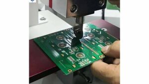
33. Manual Soldering (Rework)
Carryout rework manually as per the work instruction.
34. Re-Inspection
Verify whether rework has been carried out and parts can be released for next operation.
35. Mounting of Connectors
- Pre Tin the leads of the connector by dipping in solder bath.
- Mount the Connectors. Apply torque on screw as per the GA and clean the solder joints with IPA solution.
36. Lead forming of ICs
Form leads for IC using lead forming tool for IC, Use Tool No and Work Instruction.
37. Pre Baking Of ICs
The ICs which are to be soldered manually in isolation (which cannot be carried out reflow soldering), following procedure to be followed:
Bake the IC No.
Time started
Time completed.
38. Apply Loctite No
Apply Loctite No. where ICs is bonded to the PCB as per Work Instruction No.
Loctite No. adhesive comes in 2 parts
Adhesive (P/N)
Activator for Adhesive (P/N)
Apply Loctite by following instruction in the area between ICs and PCB.
- Bond surfaces should be clean and free from grease.
- Use applicator to apply the activator to the surface to be bonded.
- After the solvent evaporates, the active ingredients will appear wet, and will remain active for up to 2 hours after application, Contamination of the surface before bonding should be prevented.
- Apply adhesive to the un-activated surface.
- Secure the assembly, and wait for the adhesive to fix (approximately 5 minutes) before any further handling. Full cure occurs in 24 hours.
- The amount of adhesive applied to the part should ensure a minimum coverage of 90% of the area under the device and should be in contact with the bottom of the part.
- The dispensing of application of the adhesive should be done as to minimize air entrapment.
- Ensure the adhesive should not interfere with the footprint pads or the device leads.
- Shelf life of Adhesive and Activator shall be ensured.
39. Potting of Vibration Sensitive Components
Potting of vibration sensitive components to be carried out by using MIL approved RTV compound as per the process document.
40. Alignment and Spot Soldering of ICs
Ensure curing time of 24 hours is completed for the adhesive before taking up for soldering. Also, care should be taken so that the temperature on the adhesive does not cross 1250 C while soldering.
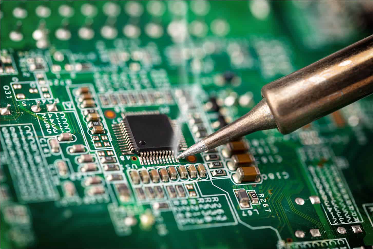
41. Manual soldering
Manual soldering of ICs under 10X magnification as per the Process Standard and Work Instruction.
42. Jumpers and Short Connections Zero Ohm Components
Solder the jumpers and Pads of Components as per General Assembly (GA) and Work Instruction. Nos. of Jumpers will be decided by designer and will be approved by RCMA with DGAQA consultation. The same will be reflected in GA drawing.
43. Cleaning
Clean the boards with IPA solution using ESD brush within 30 minutes of soldering and record soldering completion time & cleaning time.
44. Physical Inspection
- Verify the following under 40X magnification or as mentioned in the process standard.
- Soldering quality.
- Soldering defects.
- Component damage.
- Foreign Object Debary (FOD).
- QM to maintain Assembly Inspection Report.
45. Application of jet melt
Apply Jet Melt on to IC as per work instruction and record Start Time ; End Time and Shelf life expiry period.
46. Mounting of card lock
- Mount the card lock on card lock slot.
- All screw should be mounted using Loctite.
- Apply Torque as specified in process standard.
- Record Shelf life expiry period of Loctite.
47. Test as per ATP
PCBA testing has to be carried out as per ATP.
48. Screening of assembled PCBs which are having; industrial grade components
The PCBs/Modules having Industrial Grade Electronics Components shall be screened as per the JSG 0667: 2005 (Reaffirmed 2011). Following screening operation carried out:
- Stabilization bake at + 850 C for 24 Hrs.
- Thermal Shock Thermal shock at – 400 C and + 850 C with 30 minutes dwell time. Carryout for 10 cycles and ensure transfer time is 2 minutes.
- Power-on Burning PCB shall be maintained at maximum rated operating temperature with tolerance +- 50C for 48 Hrs in power ON condition and functional test to be carried out every five hours.
49. Rework
Carryout rework as per assembly inspection report.
50. Re-Inspection
Verify whether rework has been carried out and parts can be released for next operation.
51. Cleaning
Clean the PCB using ISO Propyl Alcohol (IPA) as per Process Standard (PS).
The three tank cleaning system as detailed below:
- Dip the PCB assembly in ‘Tank-1’ for 5 minutes.
- Wear antistatic gloves and clean the PCB using an antistatic brush.
- Shift the PCB assembly to ‘Tank-2’ which has in dipped condition for 3 minutes.
- Dip the PCB assembly in ‘Tank-3’ for 3 minutes.
- Dry the PCB in clean air circulated oven 55 (+/- 5)0 C.
- The solvent in Tank-1 has to be discarded when the boards failed to meet the resistivity test of solvent extract or sodium chloride salt equivalent ionic contamination test as specified in QS. Cleaning of the PCBs also can be carried using De-Greasing Machine.
52. Resistivity check
Carry out the resistivity check on one representative sample of each printed wiring board assembly type processed during each production shift. Check as per Quality Standard (QS), QM department to maintain the report/record after carrying out the test.
53. Conformal Coating Process
Mask the connectors and card lock mounting surface with masking tape and carry out Conformal Coating as per Process Standard. Record the following parameters:
Date of process; Start time; End time &Curing temperature
54. Removal of masking
Remove the masking done for conformal coating carefully without disturbing the Coating.
55. Conformal coating inspection
Verify following parameters: –
- Coating coverage (This checked under UV lamp).
- Peel off, Blow Holes and Bubbles under 4X magnification.
- Coating Thickness using the instrument.
- The masking area as indicated in the drawing is not coated with the coating material.
- Wavy pattern to be verified.
- QM department to maintain Inspection Report.
56. Functional testing
Module/PCB to be tested as per ATP and Testing department to maintain Testing Reports / Records.
57. X-ray Inspection
Carry out X-ray inspection for checking the soldering quality and to verify any shorts in the following devices.
- Integrated Circuits (ICs) including BGAs.
- Crystal Oscillator.
- Resistor Network.
58. High resolution photo
High-resolution photo is to be taken and a soft copy of the same is to be maintained by the Quality Manager (Assembly Inspection) [QM (AI)] Department.
59. PCB handling and transportation
The following procedure has to be followed for handling the PCB assemblies during transportation
- Each PCB assembly should be packed, and vacuum sealed in an antistatic aluminum foil cover with desiccant.
- Antistatic box with partition for holding one PCB assembly per partition with adequate antistatic foam or bubble sheet to give cushioning effect.
Documentation & References
All the documents used for manufacturing of the above PCB assembly including PRC to be scanned and a softcopy of the same to be maintained by the QM (AI) Department.
- Check list Kit Inspection Document.
- Production Order, General Assembly (GA), Part List, ATP for Modules / LRUs BGA.
- Part No
- Process Standards
List of documents that will be available as part of manufacturing the above PCB assembly (Data Pack)
- Kit Inspection Report.
- Screening Report of ICs.
- Reflow profiles followed for the component side and solder side.
- AOI report after reflow soldering on component side and solder Side.
- Report of visual inspection using 40X magnification.
- Inspection report after manual soldering of ICs and connectors.
- X-ray inspection report.
- Inspection report after thermal shock.
- Test reports for the tests conducted as per ATP.
- Acrylic conformal coating inspection report.
- Filled PRCs, with signature and seal of approved operators and inspectors.
- High-resolution photos of assembled PCBs (both sides) one before conformal coating and the other before dispatch.
- All AIRs pertaining to the non-conformities observed during production.
- Consolidated List of all non-conformities (NCR No. / AIR No.) observed during Material Inspection, Assembly Inspection, and testing.
- Certificate from Head, Quality Manager (QM) for having verified the disposition on Non-Conformances (NCs).
Conclusion
This document has brought out systemic procedures/practices that will help all the stakeholders to ensure Quality Assurance (QA) during Soldering Process with documentary evidence that specified quality requirements have been met.
EMSxchange Enables you to select a Printed Circuit Board, PCB Assembly, cable & wire harness assembly, and box-build suppliers meeting your Required Electronic Manufacturing Capability, capacity, and Certification Criteria from a global Electronic contact manufacturer base.
EMSxchange takes complete responsibility and ownership for your electronic manufacturing process and all its deliverables from contract manufacturing supplier selection to manufacturing to quality inspection to shipment and delivery to your door.
EMSxchange Electronic Manufacturing Partners Profile includes:
Argus Systems (AESPL) – PCB, PCBA, Cable Assembly, Box Build, Testing.