
Design for Testability Guidelines – In-Circuit Test Fixtures
1. All test targets are preferred to be on one side of the PCB.
Even though vendors are experienced and capable of equipping fixtures with top-side probing, however with bottom-side probing targeting accuracy is slightly diminished due to the additional tolerances involved.
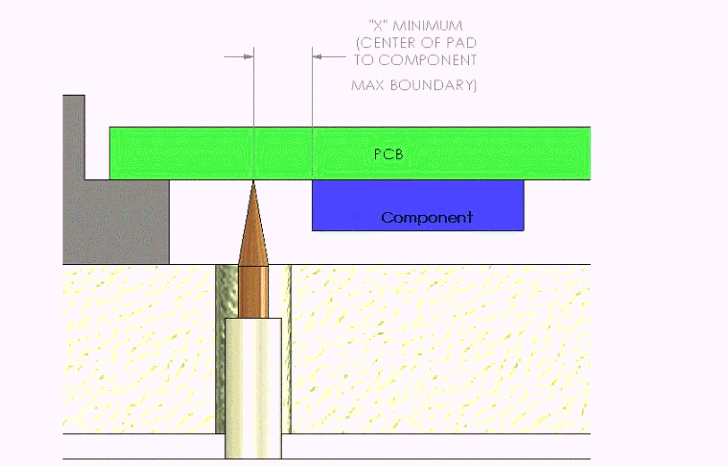
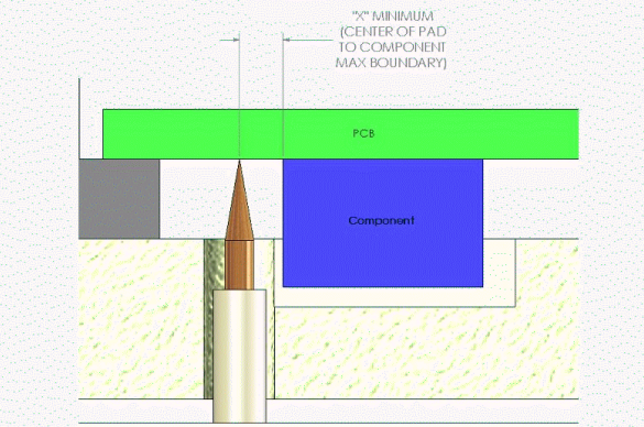
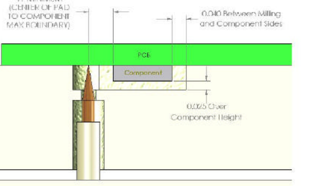
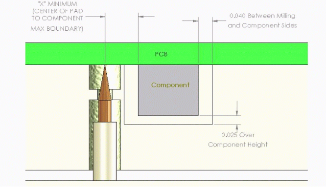
2. Test Target-to-Component Spacing
The following guidelines represent the minimum spacing allowed for placing probes relative to SMD components on the side of the board being tested. These guidelines are based on fixture drilling requirements and do not reflect any board-related keep-out requirements around the component, which may limit the spacing to a distance greater than that specified below.
In the following figures, the “component” geometry refers to the component placement boundary. Thus, all dimensions are from the edge of the component placement boundary to the center of the test target.
Note: utilize a standard clearance of .040” between the component placement boundary and milling for zero-flex top plates.
The minimum probe-to-component distances are dependent upon the pogo probe and the technology used. The situations below compare Conventional POGO Probes METRIX Probes and patented Zoom technology.
For the edge of the component to the edge of the target location, subtract ½ the diameter of the target from “X”.
| Standard Top Plate – Components under .150″ | |
| Probe Size | “X” |
| 100mil Probe | 0.0430 |
| 75mil Probe | 0.0375 |
| 50mil Probe | 0.0350 |
| Standard Top Plate – Components over .150″ | |
| Probe Size | “X” |
| 100mil Probe | 0.0580 |
| 75mil Probe | 0.0510 |
| 50mil Probe | 0.0440 |
| Zero Flex Top Plate, Guided Probe – Components Under .045″ | |
| Probe Size | “X” |
| 100mil Probe | 0.0430 |
| 75mil Probe | 0.0375 |
| 50mil Probe | 0.0350 |
| METRIX MTX-050 Probe | 0.0370 |
| METRIX MTX-039 Probe | 0.0350 |
| Zero Flex Top Plate, Guided Probe – Components Over .045″ | |
| Probe Size | “X” |
| 100mil Probe | 0.0830 |
| 75mil Probe | 0.0760 |
| 50mil Probe | 0.0690 |
| METRIX MTX-050 Probe | 0.0685 |
| METRIX MTX-039 Probe | 0.0650 |
3. Test Point Spacing
The minimum center-to-center spacing between test points or adjacent drilled locations is as follows.
From the edge of the target to the edge of the target location, subtract ½ the diameter of each target from the C/L-C/L distance listed.
Conventional Probe/Receptacle Spacing
Probe Combination Minimum Centerline Spacing
100 Mil Pogo & 100 Mil Pogo 0.083”
100 Mil Pogo & 75 Mil Pogo 0.076”
100 Mil Pogo & 50 Mil Pogo 0.069”
75 Mil Pogo & 75 Mil Pogo 0.068”
75 Mil Pogo & 50 Mil Pogo 0.061”
50 Mil Pogo & 50 Mil Pogo 0.050”
METRIX Probe Spacing
Probe Combination Minimum Centerline Spacing
MTX-050 & MTX-050 0.047”
MTX-050 & MTX-039 0.043”
MTX-039 & MTX-039 0.039”
4. Test targets should be at least .125” away from the edge of the PCB or “break away” areas.
In vacuum fixtures, this region allows gaskets to meet evenly with the board surface and create a good vacuum seal. Mechanical board handlers may require additional clearance for conveyor rails.
5. Test points should be distributed evenly over the surface of the PCB.
Areas of high probe density may cause the PCB to flex significantly, resulting in a loss of probe travel, poor probe contact with the test target, and possible damage to the PCB.
6. PCBs should have a minimum thickness of .062″ to assist in minimizing board flex.
A board stress analysis should be considered to proactively identify areas of high stress or deflection that can be addressed and corrected during fixture build. Board stress analysis predicts board flex before building the fixture.
7. The preferred lead length is .062” or less.
Avoid placing test points on excessively long leads. Additional machining may be required for long leads which could result in additional plate deflection and compromising probe contact.
8. Solder masks should not cover any test pads or vias.
9. A solder bump should exist on test pads that are recessed below the solder mask.
Ideally, and if possible, solder paste should be applied to test pads at SMT screening to promote even and consistent solder bump formation.
10. All vias should be closed.
Excessive open vias and unfilled component holes cause air leaks inhibiting the vacuum seal. Vendors can provide a mechanical hold-down gate or vacuum box in the event there are open vias on the board.
11. Avoid placing nodes on SMT devices.
This can cause damage to the device, false test results, and provides minimal probe contact area.
12. Preferred board manufacturing tolerances are as follows:
Tooling hole to pad/feature tolerance should be targeted at +/ .002”.
The diameter of the pad/feature should have a tolerance of +/- .002”.
The diameter of the tooling holes should have a tolerance of +.002”/ -.000”
13. Two tooling holes should be placed at opposite corners of the PCB.
Tooling hole diameters should preferably be .125” and should be un-plated.
Tooling hole locations should be a minimum of .100” from the edge of the PCB.
The use of diamond tooling pins should be considered to increase targeting accuracy.
14. Minimize the use of tall components on the bottom side of the PCB.
Component height greater than 0.255” creates probing difficulties and they require cutouts or relief milling in the probe plate.
Where possible extend test pads 0.200” away from tall components to allow for milling tolerances.
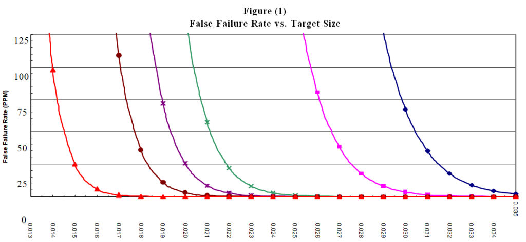
15. The preferred target size is .035”, and .040” for top side targets. The table (1) identifies fixture technology that allows for testing smaller diameter pads.
Square test targets are preferred over round.
A comparable size square pad provides 27% more target area than its round counterpart thereby improving contact reliability.
Table (1) identifies the minimum recommended target size for various types of fixtures based on a false failure rate of approximately 50 parts per million (ppm).
Similarly, Figure (1) provides a comparison of false failure rate versus target size for the various types of fixtures.
Note: The results provided in Table (1) and Figure (1) are based on the following board manufacturing tolerances: +/- .002” on the location of the test target relative to the tooling hole, +/- .002” on the diameter of the test target and + .002”/ – .000” on the diameter of the tooling hole.
| Table (1) | |
| Conventional Fixture | 0.031” |
| Conventional Fixture With Receptacle Alignment Plate | 0.027” |
| Conventional Fixture With Guided Probe Holes (Guided Probe requires Zero Flex Top Plate) | 0.022” |
| Conventional Fixture With Guided Probe Holes and Diamond shaped Tooling Pins (Guided Probe requires Zero Flex Top Plate) | 0.020” |
| METRIX Fixture (Requires Guided Probe Holes and Zero Flex Top Plate) | 0.018” |
16. Tooling Hole to Target Distance Centerline-to-Centerline
For below, X is as follows: 100mil probe: .033”, 75mil probe: .026”, 50mil probe: .019”, 39mil probe: .015”
Typically, round and diamond tooling pins have a .250” shoulder to keep them in place. This would restrict the spacing to a minimum of (0.145”+X) from centerline to centerline Tooling holes larger than .250” would be (Hole Dia/2 + 0.020” + X).
Special round and diamond tooling pins can be made to reduce the shoulder to .150” and thus the minimum spacing can be as low as (0.095”+X).
Very special pins can be manufactured to reduce further, and would ultimately be determined by the (Hole Dia/2 + 0.025” + 0.020” + X). .025” is the flange required and .020” for the web between the holes in the plate required.
Variable tooling pins require much more room to install and adjust, and thus the minimum spacing is (0.750”+X).
EMSxchange Enables you to select a Printed Circuit Board, PCB Assembly, cable & wire harness assembly, and box-build suppliers meeting your Required Electronic Manufacturing Capability, capacity, and Certification Criteria from a global Electronic contact manufacturer base.
EMSxchange takes complete responsibility and ownership for your electronic manufacturing process and all its deliverables from contract manufacturing supplier selection to manufacturing to quality inspection to shipment and delivery to your door.
EMSxchange Electronic Manufacturing Partners Profile includes:
Argus Systems (AESPL) – PCB, PCBA, Cable Assembly, Box Build, Testing.