
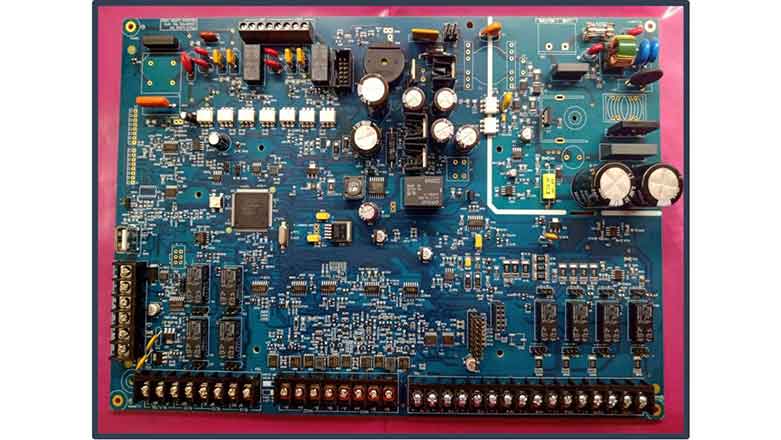
PCB Assembly Process
Electronics have become highly common in our daily lives. Miniaturisation becoming more popular in the electronics industry. All of this, however, It is made possible by the small green chips that are at the heart of all electronic devices. Yes, we’re talking about printed circuit boards, or PCBs as they’re more commonly known. The majority of these are made of fibreglass, with copper held together with epoxy and insulated using a solder mask.
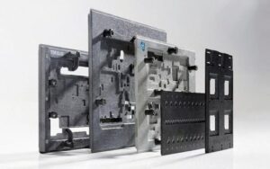
Printed circuit boards (PCBs) are the building blocks of today’s electronic devices. These PCBs are made up of a variety of small and fine components that have been carefully designed and assembled to get the desired result. As a result, PCB assembly is a simple but time-consuming operation.
It’s important not to get distracted by the process simplicity; it demands precise attention to detail. If you don’t pay attention, even the tiniest mistake might have a big impact on your performance. As a result, it’s critical to follow the PCB assembly stages precisely.
However, there are some stages that must be completed before the PCB Assembly Process may begin. This mostly entails ensuring that the PCB design is correct, which is accomplished through a Design for Manufacturability test. This is to verify that there are no operational concerns after the PCB manufacturing is completed.
A Design for Manufacturing check examines the numerous design specifications, any missing features, and other factors that could affect the PCB’s functionality. Is the space between components, for example, too small? If so, if not identified during the DFM stage, it could lead to short circuits later. DFM can thus help to ensure that costly errors are avoided in the future.
Before going directly to the Printed Circuit Board assembly process let’s learn basic things about PCB.
PCB Layers and Design
There are multiple signal layers between the outer layers. Let’s discuss on the types of outer layers and functionality.
1) Substrate
This is the rigid FR-4 board that the components are “stuffed” or soldered onto. This gives the PCB its rigidity.
2) Copper Layer
To generate top layer and bottom layer copper traces, thin copper foil is put to the top and bottom of the PCB.
3) Solder Mask
It’s the layer that goes on the top and bottom of the PCB. This is used to make a non-conductive region on a PCB and to protect short circuits by isolating copper lines from one another. The solder mask also prevents soldering on undesirable areas and ensures that solder only travels where it’s supposed to go, such as holes and pads. THT components will be attached to the PCB through the holes, whereas SMT components will be held in place by the PADs.
4) Silk Screen
The white labelling on PCBs for component designators such as R1, C1, or any form of description on the PCB or company logo is all constructed of silk screen layer. This silk screen layer contains all of the necessary information regarding the PCB.
Types of PCB
1) Rigid PCB
Rigid PCBs are the majority of the PCBs we find in various types of gadgets. These are PCBs that are hard, rigid, and solid, and come in a variety of thicknesses. Fiber glass, or simply “FR4”, is the primary component. “Fire Retardant – 4” is what FR4 stands for. Because of its self-extinguishing properties, FR-4 is ideal for usage in a variety of hard core industrial electronic equipment. Copper clad laminates are made by laminating two sides of FR-4 with a thin layer of copper foil.
Power amplifiers, switch mode power supply, servo motor drives, and other applications use FR-4 copper clad laminates. Paper Phenolic PCB, on the other hand, is a hard PCB substrate that is extensively utilised in home appliances and IT devices. They are light in weight, low in density, inexpensive, and simple to punch and drill. Calculators, keyboards, and mice are just a few of the devices it can be used with.
2) Flexible PCBs
Flexible PCBs are constructed using a substrate material called Kapton, which can endure extremely high temperatures and has a thickness of only 0.005 inch. They can bend readily and are utilised in wearable electronics, LCD display or laptop connectors, keyboard and camera connectors, and other applications.
3) Metal Core PCBs
Alternatively, another PCB base material, such as aluminium, can be utilised, which is excellent at dissipating heat. These PCBs can be utilised in applications that require heat-sensitive components such as high-power LEDs and laser diodes, etc.
Types of PCB Assembly Technology
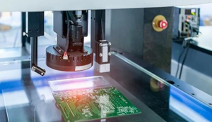
1) SMT (Surface Mount Technology)
SMT components are very small and come in a variety of packages for resistors and capacitors, such as 0402, 0603, and 1608. Similarly, we have SOIC, TSSOP, QFP, and BGA for integrated circuits.
Since SMT component assembly is complex and time consuming for human hands, it is mostly done by automated pick and place robots.
2) THT (Through Hole Technology)
Resistors, capacitors, inductors, PDIP ICs, transformers, transistors, IGBTs, and MOSFETS are examples of components with leads and wires.
The component must be put on one side of the PCB and pulled to the other side by the leg, which must then be cut and soldered. The assembly of THT components is often done by hand soldering and is relatively simple.
Printed Circuit Board assembly process
- Solder Paste Printing
The foundation step of PCB assembly is solder paste stencilling. This phase is the same regardless of the kind of PCB construction. Over the board, a stencil composed of a thin metallic sheet is laid. It guarantees that the solder paste is only applied where the components will be installed. The stencil is removed from the board once solder paste has been applied.
- Pick and Place Components Mounting
Component mounting is a select and place action that can be done manually or mechanically by an automated system. The component mounting is done manually in the through-hole PCB assembly. The construction of surface-mount PCBs is done by an automated machine. The technique of automatic component installation is quick, precise, and error-free.
- Soldering
Soldering is used to connect components on a printed circuit board. Wave soldering is used in the through-hole assembly process. The PCB with attached components passes through a hot wave solder liquid in this process. This liquefies the solder balls, which solidifies the paste when it cools to room temperature. Reflow soldering, on the other hand, is used in surface mount PCB assembly. The PCB is run through a furnace that is heated to 500°F in this process. The solder paste melts and settles with the components as it cools.
- Inspection
Inspection and quality testing are carried out to guarantee that the item works properly. It entails three separate inspection procedures, which are detailed below.
- Visual/Manual Inspection
Only the soldered connections need to be inspected manually. This approach is only suitable for small batches of PCBs; otherwise, it loses accuracy due to optical fatigue.
- Automatic Optical Inspection (AOI)
To examine PCBs, the AOI machine has high-resolution cameras that can be aligned in various angles. This sort of examination is appropriate for single and double-sized PCBs, but not for multi-layer complicated PCBs.
- X-ray inspection
Intricate PCB designs with multi-layer component mounting are subjected to X-ray inspection. Optical inspection of such complicated PCBs is difficult.
- Post Assembly Inspection and Functional Testing:
After assembly, the PCBs are inspected and functionally tested. To complete the process, functionality tests such as micro-sectioning, contamination, and solderability are done.
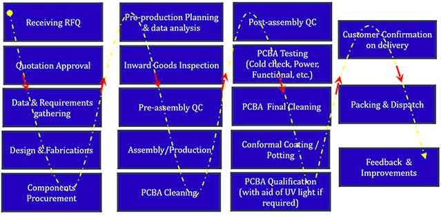
PCB Assembly Process Flow
EMSxchange Enables you to select a Printed Circuit Board assembly suppliers meeting your Required PCBA Manufacturing Capability, capacity and Certification Criteria from a global PCB Assembly manufacturer base. EMSXchange takes complete responsibility and ownership for your electronic manufacturing process and all its deliverables from contract manufacturing supplier selection to manufacturing to quality inspection to shipment and delivery to your door. EMSxchange Electronic Manufacturing Partners Profile includes:
Argus Sytems (AESPL) – PCBA, Cable Assembly, Box Build.
Cerra Systems inc – PCB Manufacturing.