
What is PCB Stencil?
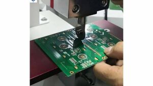
PCB Stencil is a sheet of stainless steel with laser-cut apertures that is used to apply solder paste to a PCB board for the insertion of surface mount components. The PCB stencil is used to apply solder paste to specific areas on a bare PCB board so that components can be precisely fitted and aligned.
Its major purpose is to precisely deposit the correct amount of solder paste on SMT pads so that the electrical connection and mechanical strength of the solder joint between the pad and the component are excellent.
The PCB Assembly process is sped up by using a PCB Stencil to apply solder paste. It also makes applying solder paste more precise.
SMT stencil manufacturing processes.
When it comes to PCB stencils, nickel or stainless steel is the most common material. As a result, stencils can be classed according to the manufacturing process used. Please keep in mind that the aperture development process for the stencil is the most important part of the production process. The procedure may include one or more of the following steps.
Chemical Etching
It is a naturally subtractive method that involves a chemical etching procedure to create apertures. It is a reasonably inexpensive method, although it usually produces inferior results.
Advantages:
- It is capable of withstanding any known and regular cleaning process.
- It is reasonably priced.
- One-time molding
Disadvantages:
- It is quite slow.
- Apertures with rough sidewalls can result from this technique.
- It is also harmful to the environment.
- Not enough accurate.
- Gradually eliminated.
Process flow:
PCB data file → film production → exposure → development → etching → steel sheet cleaning
Laser Cutting
It’s also available as a subtractive method, in which the stencil foil is removed via laser cutting. By default, laser cutting produces a finer output and aids in achieving higher accuracy. When opposed to chemical etching, it also produces more consistent output or outcomes. It’s worth noting, however, that the process is unaffected by the chemical environment and hence does not require moisture protection.
Advantages:
- Slots with a tapered shape
- It is faster than other stencil-making methods, such as chemical etching.
- Film tooling isn’t present.
- Precision cutting can be done
Disadvantages:
- The sidewalls of the aperture are rough.
- It needs an extra deburring process.
- The production speed is slower.
Electroforming
It is an additive method that involves nickel electroforming to generate the stencil foil. E-FAB is another name for the procedure. While the technique has a significant upfront cost, the price is frequently unrelated to the aperture number. In this manufacturing or fabrication process, a longer processing time is also considered a disadvantage.
Advantages:
- Available in a variety of thicknesses.
- Slots with a tapered shape.
- Exceptional accuracy.
Disadvantages:
- Increased processing time.
- The price is too high.
- High start-up costs.
- It necessitates film tooling.
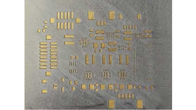
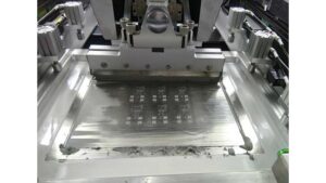
Types of the PCB Stencil
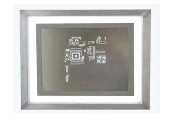
Fig 1: SMT stencil with frame
Fig 2: Micro stencil
Stencils are divided into the following types based on solder paste application:
The Framed SMT Stencil
Frameless SMT Stencil
This sort of stencil, also known as foil, is made up of laser-cut stencils that are meant to work with reusable stencil frames known as stencil tensioning systems. It’s an SMT stencil, which means it doesn’t need to be permanently glued into the frame. In comparison to framed stencils, frameless SMT stencils are less expensive. In addition to supplying enhanced quality and higher performance, it also saves money in terms of storage.
SMT Stencil Electroformed
It’s a stencil made of nickel. A mesh border permanently mounts the electroform SMT stencil or electroformed foils on a stencil frame, securely stretching the foil taught within the frame. Electroformed stencils provide some of the best paste release properties on the market. As a result, it is used in fine pitch SMT applications on PCB boards (12 mil to 20 mil pitch). It’s also useful for flip chips, wafer bumping, and BGAs (6 mil to 12 mil pitch).
Prototype SMT Stencil
It is a type of laser-cut stencil that is manufactured to order from your CAD or Gerber files. In this situation, the stencil must match the PCB prototype created. The PCB stencil producer creates frameless solder paste stencils exclusively for hand printing. Because of its unique character, it must be printed by hand.Stencils are divided into the following types based on solder paste application:
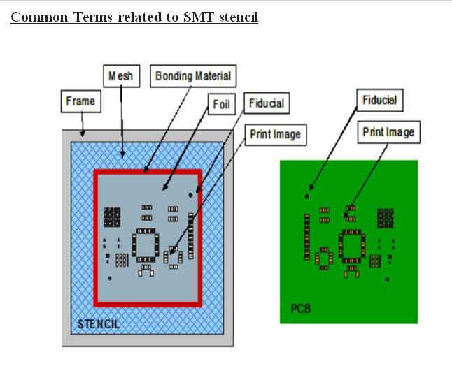
Fig 3: Terms related to stencils
Aperture:
An opening in the stencil which is designed slightly smaller than the PCB pad size. We can apply solder paste through this so that right amount of solder paste can be accurately deposited on SMT pads. Common shapes include rectangles, squares, rounds etc.
Fiducial:
Fiducials are alignment marks that is used to align the bare pcb with stencil.
Frame Size:
Foils are permanently mounted into aluminium frames to provide optimum solder paste volume control. Typical frame size is 29″ X 29”.
Foil Thickness:
Foil thickness can be decided as per the amount of solder to be deposited on pads through opening.
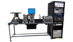
EMSxchange Enables you to select a Printed Circuit Board assembly suppliers meeting your Required PCBA Manufacturing Capability, capacity and Certification Criteria from a global PCB Assembly manufacturer base. EMSXchange takes complete responsibility and ownership for your electronic manufacturing process and all its deliverables from contract manufacturing supplier selection to manufacturing to quality inspection to shipment and delivery to your door. EMSxchange Electronic Manufacturing Partners Profile includes:
Argus Sytems (AESPL) – PCBA, Cable Assembly, Box Build.
Cerra Systems inc – PCB Manufacturing.