
PCB Thermal Management – Thermal Via
- To operate efficiently and ensure reliability, heat must be removed from heat-generating power components.
- As a result of faster speeds, reduced format, and more devices being populated on PCBs, more heat is being generated that must be removed for efficient operation.
- The move to sustainable energy increased the demand for energy management electronics which also create much heat because of the high electrical currents used on these applications (Power inverters for solar and wind energy, powertrain electronics for HEV)
- Thermal management through various applications aids in directing heat away from heat-generating system components.
Thermal Conduction In PCBs

Thermal Management Types Offered

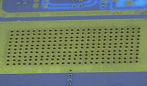
Thermal Vias
Thermal vias are the most easily produced form of thermal management
- Thermal vias or ‘via farms’ are tightly grouped vias that are patterned and located under heat-generating devices.
- They are the least efficient for heat removal but are cost-effective for devices with low power and heat generation.
- The vias can be plated with an additional copper thickness (1.5 to 2.5 mils) to enhance the thermal conduction of the heat from the device through the board to a secondary heatsink or chassis.
- This process will add cost and may affect outer layer feature capability.
- Disadvantage – when attaching components soldier tends to flow through the vias.

Double-sided or multi-layer PCB

Holes drilled. As part of the drill process, the thermal vias or via farm are produced in a tight pattern in the required location.

Thermal vias are plated along with the other required holes. In some cases the thermal vias may be plated with thicker copper to enhance thermal heat transfer.

If GND planes are connected to the Thermal vias, they will act as a ‘heat-spreader’ which will further improve the heat transfer and reduce the ‘hot-spot’.
Thermal Vias


Hot Spot Cooling Thermal Via and Heatsink

Component side

Heatsink side
How to avoid Solder flowing through the thermal-vias
Modify solder mask and solder-paste stencil

Min DHS = 0.35mm to avoid blocked holes
Soldermask Plug for Thermal Vias

Only to use with ENIG (or HASL) as it is a thermally cured ink applied after the surface finish
Cap-plated Epoxy-filled Via

Expensive option with a huge impact on process flow and design-rules.
Vias Resistance vs Length

Thermal Resistance: Parallel Thermal Vias

Method to Increase Thermal Via Conductivity

Thermal Resistance vs Via Technologies

EMSxchange Enables you to select a Printed Circuit Board, PCB Assembly, cable & wire harness assembly, and box-build suppliers meeting your Required Electronic Manufacturing Capability, capacity, and Certification Criteria from a global Electronic contact manufacturer base.
EMSxchange takes complete responsibility and ownership for your electronic manufacturing process and all its deliverables from contract manufacturing supplier selection to manufacturing to quality inspection to shipment and delivery to your door.
EMSxchange Electronic Manufacturing Partners Profile includes:
Argus Systems (AESPL) – PCB, PCBA, Cable Assembly, Box Build, Testing.