
Introduction
- Present the cost impact of many PCB design attributes.
- Conveys trend data only (does not represent the entire process for establishing the price of PCBs).
- Help to provide some guidance on attribute selection during the design phase of the product.
- Provide the realization that PCBs are custom designed and require early supplier involvement to achieve the most cost-effective product.
- Cost factors relate to the panel, not piece cost
- Shall not be used for pricing or quote compare
General Information
- Historically the industry has been able to gain cost reductions by transferring products across the globe. In order to remain competitive moving forward, we must work together to design for optimum cost-effectiveness.
- EMSxchange brings value in understanding that PCBs are custom products whose costs are driven by a multitude of different attributes including; size, material, technology, etc., and our technical involvement can help to minimize the impact of these costs on the final product.
- All data shown in this presentation reflect average price adders to illustrate trends as attributes are changed.
- Data in all the charts are derived from the following product conditions:
- Standard Mid Tg FR-4 Material5 mils lines & spacing.025” SMT pitch.014” Drill DiameterAverage 50 holes/sq. in.
- OSP/HASL
Cost Breakdown
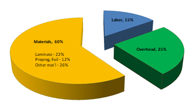
- Below is the approximate cost breakdown for multilayer PCBs in Asia.
- Labor continues to increase as a percentage of the total cost.
What Factors Drive PCB Cost?
- Manufacturing panel utilization (how PCBs fit on a master panel)
- Layer count
- Basic process complexity, including minimums/maximums for:
- Line and space
- Drilled hole size / Aspect Ratio
- Overall PCB thickness
- Annular ring requirements
- Copper weights etc.
- Exotic process operations (via-in-pad, buried capacitance, buried resistors, castellations, milling, etc.)
- Choice of materials
- Performance class (IPC 6012B Class 2/3/3A, MIL-PRF-31032, …)
Layer to Layer Differential
| 2 to 4 | 42% | Mass Lam |
| 4 to 6 | 22% | Mass Lam |
| 6 to 8 | 14% | Mass Lam |
| 8 to 10 | 19% | Pin Lam |
| 10 to 12 | 16% | Pin Lam |
| 12 to 14 | 13% | Pin Lam |
| 14 to 16 | 11% | Pin Lam |
| 16 to 18 | 10% | Pin Lam |
| 18 to 20 | 10% | Pin Lam |
This illustrates the cost impact as you increase from one layer count to another. All other product attributes are assumed to be identical. A medium-complexity product was used for comparison purposes.
Laminate Types
| Tier | Classification | Df range | Example materials | Data Rate (Gbps, typical range) | Relative Laminate Cost (X-Factor) |
| 4 | Ultra Low Loss | <0.0050 | Megtron 7N, TU-933, DV(N), etc. | 25.0-50.0 | 3.8-7.0+ |
| 3 | Very Low Loss | 0.0050-0.0099 | Megtron 6G/6K, DS7409DV, etc. | 12.5-25.0 | 2.8-5.0 |
| 2 | Low Loss | 0.0100-0.0149 | Megtron 4, EM-888, etc. | 6.125-12.5 | 1.5-2.0 |
| 1.5 | Mid Loss | 0.0150-0.0200 | Megtron 2, EM-370D, TU-862HF, etc. | 3.0-6.125 | -1.0 |
| 1 | Standard Loss | >0.0200 | -370HR, R-175SV, etc. | <3.0 | 1.0 |
Laminate Types
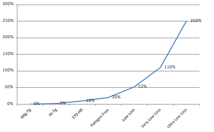
This data reflects the cost impact of different raw materials for a 16-layer board and takes into consideration the variation in processing costs and yield implications.
Copper Thickness – Internal
Inner Copper Weight Impact
| Copper Weight (oz) | 2 | 3 | 4 | 5 | 6 |
| Cost Impact % | 30.0% | 80.0% | 105.0% | 150.0% | 190.0% |
This estimation includes higher copper etching cost with thicker copper, and extra resin in prepreg for heavier inner copper material.
Copper Thickness – External
Outer Copper Impact
| Outer Copper | 0.25 | 0.33 | 0.5 | 1 | 2 |
| 6L | 0.0% | 0.0% | 0.0% | 0.0% | 12.0% |
| 16L | 0.0% | 0.0% | 0.0% | 0.0% | 6.0% |
Increased processing costs are reflected in the data for 2 oz.
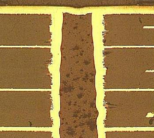
Internal Layer Line Width & Spacing
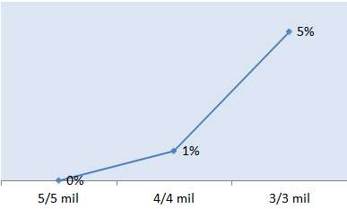
This data takes into consideration the variation in processing costs and yield implications. This is a reference to 1 Oz or below base copper. The thicker base copper adder is higher
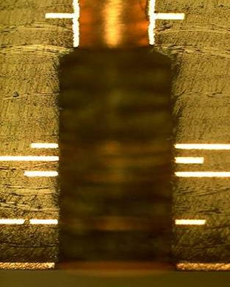
Outer Layer Line Width & Spacing
This data takes into consideration the variation in processing costs and yield implications. This is a reference to half Oz base copper. A thicker base copper adder is higher.
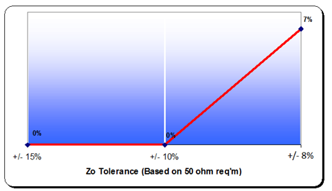
Board Thickness Tolerance
- </= 0.050” thick (+/- 15%)
- >0.050” thick (+/- 10%) = Baseline
- >0.050” thick (+/- 8%) ~ 3 – 5% cost add
- <8% tolerance; capability and cost are dependent on design
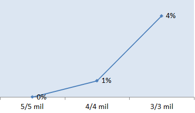
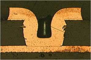
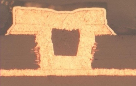
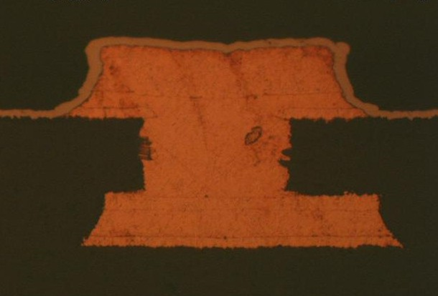
Minimum Finished Hole Size
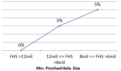
This data reflects the minimum drilled hole size in a .062” thick PCB. Products thicker than .062” thick will increase the cost.
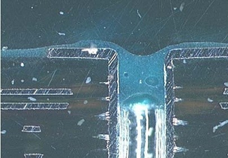
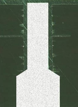
Thru-hole Drilling/Aspect Ratio
- Standard Thru-hole: Typically >/= .014” dia. drill
High Aspect Ratio

Hole Aspect Ratio
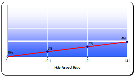
Since aspect ratio is not linear this data reflects aspect ratios within our capabilities.
Average Hole Density
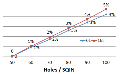
This data solely reflects the cost implications of increasing the average number of holes per square inch.
Controlled Impedance
Cost factors and tolerances are based on a nominal impedance value of 50 Ohms. Standard working tolerance is + 5 ohms or 10%, whichever is greater. Additional costs will be incurred if 100% testing is required.
Surface Finishes
| HASL | OSP | Immersion Silver | Immersion Tin | ENIG | |
| 2L | 8% | 0% | 0% | 2% | 14% |
| 10L | 5% | 0% | 0% | 1% | 8% |
Data reflects the cost impact of surface finishes after solder mask application. (Low market demand on HASL cause high running costs)
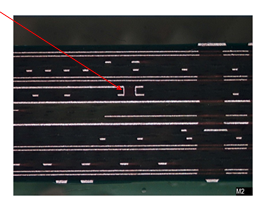
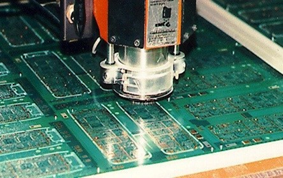
Panelization / Array Design
- Optimizing the part and/or array size for best panel utilization can improve cost by as much as 40%
- Non-usable border requirements may vary between facilities and can be affected by design attributes
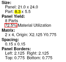
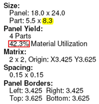
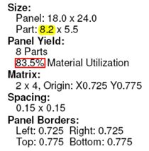
You are paying for the panel regardless of the pieces up
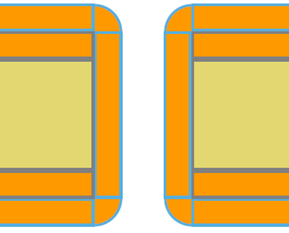
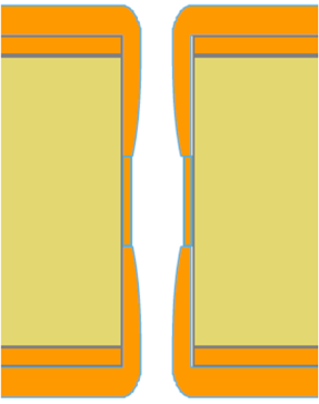
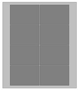
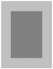
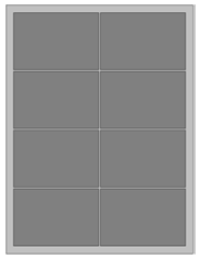
Panelization / Array Design
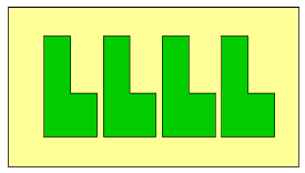
4 per Array

8 per Array
Array Design
Design to meet assembly process requirements
Questions to ask/answer:
- Minimum part dimensions (smallest part) that can be run through the assembly process?
- Maximum part dimensions?
- Are rails required?
- Rails on how many sides?
- Minimum rail width required?
- Are tooling holes allowed to be added to rails and are there limitations to distance from the active part edge?
- Is the addition of external and internal copper thieving allowed on rails?
- Are “X-outs” allowed on multi-part arrays and what are the limitations?
Panelization / Array Design
Notes:
- Inactive border growth can occur if the addition of special coupons is required.
- Excessive impedance measurement requirements can have the potential to grow coupon space needs.
- The above does not cover all interactions.
- If we can improve penalization from the above on a particular design, we will.
Panelization
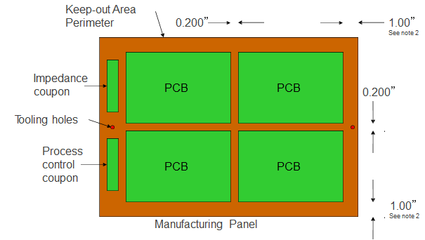
Note: 1-Depanelization space can be as small as 0.100” and if board geometry permits scoring can be used
2- Borders can be as small as 0.750”
Soldermask and Legend
- Soldermask colors
- Green = Baseline
- Other colors ~ 2% cost add
- Legend / Nomenclature
- Legend on both sides (default) = Baseline
- No Legend ~ 1% cost reduce
Via Treatments
- Via Cap
~3% cost add
- Soldermask via plug
~5% cost add
- Soldermask via fill
~5% cost add
Plated overfilled via
~$20 -$40 cost added per panel (for Through Holes)
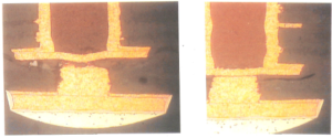
Buried Plated Cores
- Drilled and Plated Buried Cores
~30% cost add to panel per core
- Based on 10 layer board
- Does not account for margins and yield
- Thin core processing (<10 mil) is likely higher
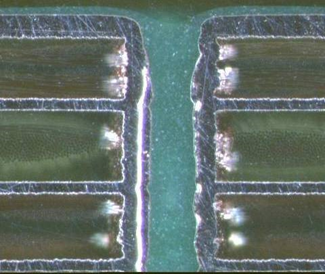
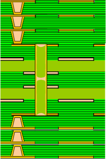
Controlled Depth Drilling
- Laser Drill Micro-vias
~10% – 14% cost add
- Backdrilling (Stub Removal)
~5% – 10% cost add
- Backdrilling with Non-conductive Fill
~ 20% cost add
Does not include the cost of micro via formation
- Non-conductive fill with plated cap
– ~10% – 20% cost add
Micro-vias plated full
– ~10% – 20% cost add
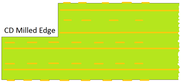
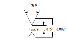
Mechanical Finishing (Sizing)
- Rout Profile
- (+/-) 0.005” tolerance = Baseline
- (+/-) 0.004” tolerance ~ 1% cost add
- Rout + “V-score” ~ 1% cost add
- Edge milling rails ~ 2% cost add
- Single lamination Baseline
- Sequential – 2 Laminations ~ 66% cost add
- Sequential – 3 Laminations ~ 130% cost add
- Sequential – 4 Laminations ~ 200% cost add
Sequential cycles add material and process steps such as lamination, drilling, plating, print & etch and others, as well as increase yield loss.
Conclusion
- Early Supplier Involvement (ESI) will facilitate minimizing cost adders at the product conceptual stage thus contributing to cost improvement for the life of the product.
- Emsxchange brings value in understanding that PCBs are custom products and our technical involvement can help to minimize the impact of costs on the final product
- The model baseline will move as technology requirements continue to rise. This is indicative of a very dynamic PCB industry.
EMSxchange Enables you to select a Printed Circuit Board, PCB Assembly, cable & wire harness assembly, and box-build suppliers meeting your Required Electronic Manufacturing Capability, capacity, and Certification Criteria from a global Electronic contact manufacturer base.
EMSxchange takes complete responsibility and ownership for your electronic manufacturing process and all its deliverables from contract manufacturing supplier selection to manufacturing to quality inspection to shipment and delivery to your door.
EMSxchange Electronic Manufacturing Partners Profile includes:
Argus Systems (AESPL) – PCB, PCBA, Cable Assembly, Box Build, Testing.