
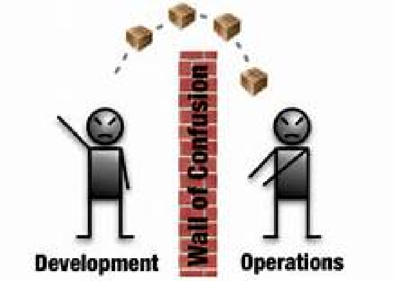
Avoid Throwing Your Design Over the Wall
Not Every PCB Shop Are Created Equal
- Define migration path from Prototypes to Final Fabrication and approve stack-up with Final Fabrication site(s)
- Design in accordance with Standard Capability DFM guidelines
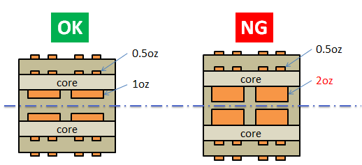
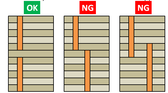
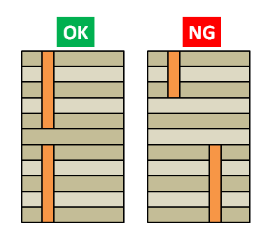
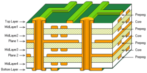
Symmetric Stack-up
- Using a symmetric (or balanced) stack-up is the most important step that can be taken to ensure that no warpage or residual stresses are present in the final product.
- The build should be symmetrical about the z-axis, including copper, prepregs, and cores.
- Either core or prepreg or copper is thicker on one side only.
- Unbalanced copper thickness on a core is feasible only when the difference is small (i.e. 0.5oz and 1oz)
- Still need to keep the overall stack-up balanced.
Via Configuration
- Keep it simple
- Mechanically drilled holes cannot be overlapped
- Also need to consider balancing
- Do NOT stack laser vias over buried vias – high-reliability risk!
- Use staggered vias instead
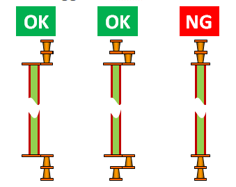
- Very high chance of separation after Thermal Stress or Reflow
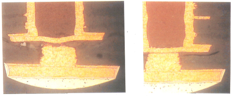
Z-axis expansion failures after Thermal Stress
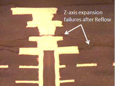
Z-axis expansion failures after Reflow
Tear Dropping
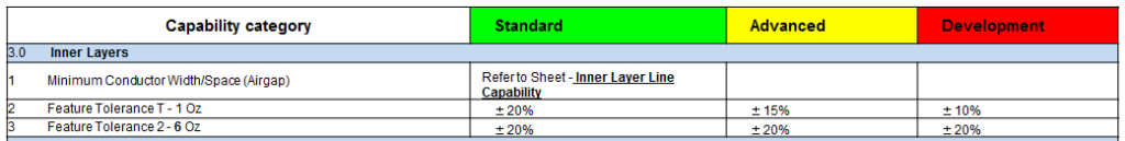
- IPC Class 2 specification allows up to 900 hole break-out.
- In order to improve manufacturing yield, ‘tear drops’ shall be added to the trace/pad junction.

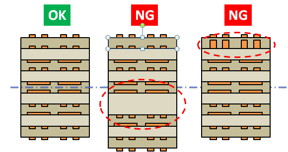
Copper Balancing (Thieving)
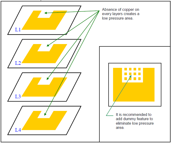
- Avoid having an unbalanced pattern on the inner layer. Otherwise, there is a risk of creating a low-pressure area during lamination. It is recommended to add a dummy copper feature to facilitate lamination.
Isolated Features
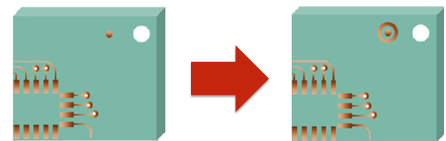
With fiducials that are isolated and away from other copper features, plating current density will be higher resulting in thicker and uneven surfaces. Etching uniformity can also be affected causing unbalanced etching. Therefore, it is recommended to add a copper ring around such fiducials. The ring can be covered with a solder mask.
DHS vs FHS
- Designers mostly care about Finished Hole Size (FHS) but PCBs only care about Drill Hole Size (DHS)
- DHS is used in design rule considerations:
- Hole-to-copper distanceHole (wall) to hole (wall) distance for CAFAnnular ring
- Plating aspect ratio
- Typically, DHS = FHS + 4mil (100um) but can range from + 3mil (75um) to + 6mil (150um) depending on aspect ratio, copper thickness, etc.
- Suggest FHS tolerance to be + 3mil (75um) / – Hole Size
Press Fit Holes
- When dealing with press-fit holes, it is best to specify FHS (with its tolerance, which is usually +/-2mil) only.
- Some press-fit connector manufacturers may also specify the drill size, surface finish, and copper plating thickness within specific tolerances. But due to actual board design, such conditions may not be realistic.
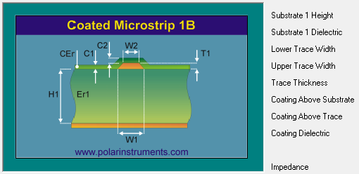
Just Follow the Stack-up Exactly!
- Basically ok (if no impedance involved) BUT…
- Availability of Resin Content (and sometimes Glass Style) may be different from region to region
- If impedance is required, then need to consider different Dk values. We uses internal Dk values for most of the existing materials (rather than databank) to get a more accurate simulation
- Upper trace width will vary from site to site depending on the process set up
- Also, solder mask type and coating thickness will affect the impedance
EMSxchange Enables you to select a Printed Circuit Board, PCB Assembly, cable & wire harness assembly, and box-build suppliers meeting your Required Electronic Manufacturing Capability, capacity, and Certification Criteria from a global Electronic contact manufacturer base.
EMSxchange takes complete responsibility and ownership for your electronic manufacturing process and all its deliverables from contract manufacturing supplier selection to manufacturing to quality inspection to shipment and delivery to your door.
EMSxchange Electronic Manufacturing Partners Profile includes:
Argus Systems (AESPL) – PCB, PCBA, Cable Assembly, Box Build, Testing.