
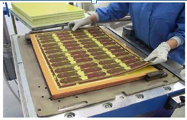
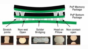
Lay-up
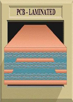
Inner cores and prepregs are stacked together in order as per the ML construction. The operation of creating the stack is called ‘Layup’.
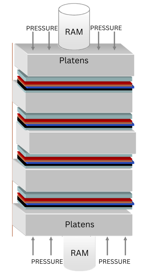
Need for Pressing
Pressing is needed to bond individual layers when there are more than 2 layers. It is also called as multilayer lamination
The layers are bonded by applying high temperature and high pressure.
Layup Process
In this process, all the input materials such as inner cores, prepregs, and copper foils are placed together on a stack with other consumables such as kraft papers, SS plates & Aluminum foils.
The tooling pins decide the height of the stack and the caul plates decide the position
LAY UP ENVIRONMENT
- Positive air pressure
- Source of filtered (5 microns) air
- Daily cleaning of the room
- Clean protective gloves & lint free lab coats and caps for operators
- Controlled temperature & humidity (20+-2 deg C, 50% RH )
- Precleaned lamination fixtures and other accessories
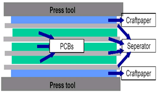
The panel layups are stacked together to form a ‘Book’.
A Book comprises 10 panels.
Aluminium sheets (Duo foil) are used between the individual layups to protect the copper foil surface and ensure that the layups do not stick together.
Prepregs are glass cloth impregnated with resin. The prepreg provides the bonding material between the layers. The heat and pressure cause the prepreg to flow and bond to the surface of the inner layers during the pressing operation.
The press applies heat and pressure to the stack so that the thermosetting resin in the
Flash trimming
After pressing the flash needs to be removed and the panels need to be brought into the standard size. This is done by the process of Flash Trimming
X-ray
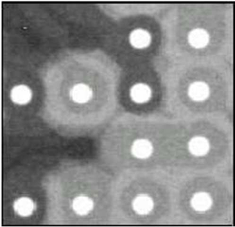
After flash trimming, the panels are measured in an X-ray machine on a sampling basis to measure the expansion or contraction of the inner layers. This measurement is done in order to decide on the drill program that needs to be used in order to drill holes at the center of the inner layer pads.
PCB Drilling
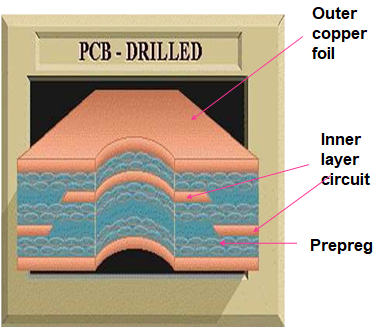
The Drilling process creates a path for making contact between different layers. The drilled hole is plated with copper for this purpose.
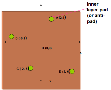
Inner layer pad (or anti-pad)
The co-ordinates for the drilling program are given by taking the center of the panel as the origin (Coordinate system)
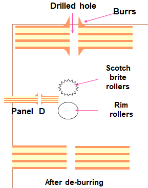
De-burring
During the drilling operation, burrs will be created around the drilled holes. The burrs are nothing but the projection of the copper from the surface. The burrs are removed by passing the panels in-between scotch bite rollers.
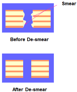
De-smear
While drilling the temperature inside the hole rises up to 600 degree centigrade. Because of this the prepreg melts and accumulates on the walls of the drilled hole. This deposition of molten prepreg on the walls of the hole is known as a “smear”
The smear is removed by treating the panels with conditioner (a sodium hydroxide-based chemical) and Sodium permanganate solutions.
PCB Plating techniques
Electro less Plating
Electroless plating is a method to plate metal onto metals or non-metals without the aid of electric current but through chemical reduction
Electrolytic Plating
Electrolytic plating or electroplating is a method to plate metal onto metal with the aid of electric current (DC or AC) through electron transfer.
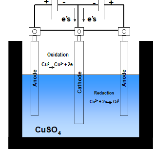
Principle of Electrolytic Plating
The basic electroplating cell is a tank containing copper salt solution in which the cathode and anode are immersed. Both anode and cathode are connected to a Power source.
The copper deposition at the cathode involves the reduction of ionic copper to metallic copper.
Copper anodes are dissolved (Oxidized) to replenish the copper concentration in the solution.
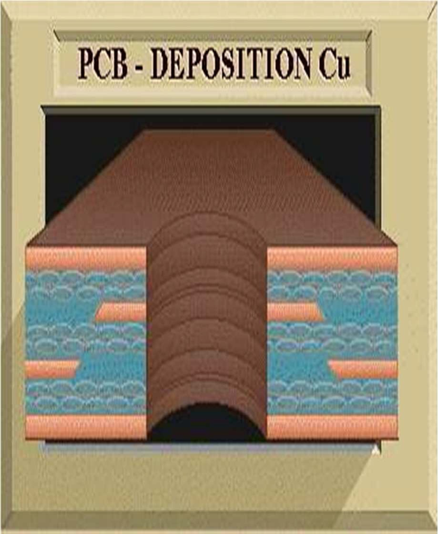
Plated through hole (PTH)
In PTH (Electroless Plating) process, the holes are made conductive by platting copper on the walls of the holes, to provide an electrical connection between the layers.
Activator: After chemically cleaning and micro-etched, the panels are treated with Stannous Chloride and palladium chloride. At the end of this process, a thin layer of palladium chloride (conducting) is formed along the walls of the holes.
Production- Flow (PTH)
Electroless Cu plating
The panels are then treated with an alkaline solution containing Copper sulfate, formaldehyde, and EDTA with other organic additives. At the end of this process, a thin film of chemically reduced copper (of thickness 5m) is applied onto the activated surface.
Reverse Pulse plating (RPP)
RPP is a typical example of AC Electroplating.
In Pulse Plating Reversal Current, the cathodic plating current is disturbed and reciprocated i.e. turned anodic for a short time.
Hole wall after activation
The anodic (= Reverse) current causes certain molecules to drift. The additives in the solution are then attracted to the high current density areas and adsorbed on the PCB’s surface. The adsorbed additive on the copper surface acts as an insulator, it will shield the current and thus temporarily prevent copper from being deposed during the Forward pulse.
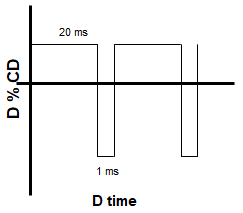
During the Forward Pulse, copper is deposited everywhere on the Printed Circuit Board – – most on the hole entrances and less in the middle of the barrel. The Forward current is nothing more than a single pulse in D.C. and the deposit is ‘dog boned’.
When the Reverse Pulse comes, the additive is attracted (‘electroplated’) to the edges of the drilling hole. Because the Reverse Pulse is also a kind of pulsed D.C., the additive layer is dog boned too
During the first phase of the next Forward Pulse, the unshielded areas are electroplated, and the organic layer is partially removed.
During the last phase of the forward pulse finishes the electro-deposition without dog-boning. (The light-blue-colored area).
Outer Layer Photoprinting
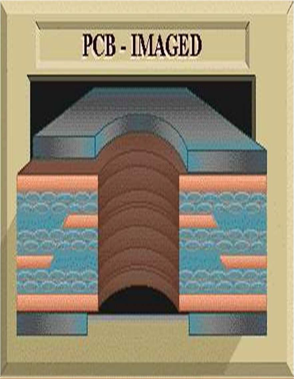
Photo printing is an image transfer process. It consists of surface preparation (pumice scrubbing), lamination, exposing, and developing processes similar to inner layer image transfer processes.
EMSxchange Enables you to select a Printed Circuit Board, PCB Assembly, cable & wire harness assembly, and box-build suppliers meeting your Required Electronic Manufacturing Capability, capacity, and Certification Criteria from a global Electronic contact manufacturer base.
EMSxchange takes complete responsibility and ownership for your electronic manufacturing process and all its deliverables from contract manufacturing supplier selection to manufacturing to quality inspection to shipment and delivery to your door.
EMSxchange Electronic Manufacturing Partners Profile includes:
Argus Systems (AESPL) – PCB, PCBA, Cable Assembly, Box Build, Testing.