
LDI helps Elimination of Photo Tools
- No Film/Artwork Movement
- Quick Turn Made Easy
- Run product as soon as Engineering releases data to the floor
- Reduction in Defect Count.
- Direct Write = No Film-related defects
- No issues related to loss of vacuum
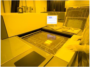
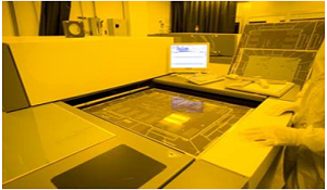
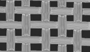
Scanning Optics
- Improved Resolution
- System Resolution 4000 dpi
- System Capability: 50µm/50µm (0.002”/0.002”) Line & Space
- Improved Registration
- CCD Camera System & Target Fiducials
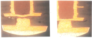
- Through Holes Drilled
- 24 Hole Pattern of Laser Drilled Microvia
- System capability
- Positional Accuracy +/-25µm
- LDI Solder Mask
- Taiyo LDI SM
Using CCD Cameras and Mechanical or Laser Drilled Fiducials it is possible to get perfect registration every time.
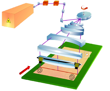
Laser Drilling Technology Overview
- Hole diameters range from 4 to 8 mils and are typically in the 5 to 6 mil range
- Hole depth is limited by copper plating aspect ratio, typically 0.5: to 0.6:1 however higher aspect ratios can be achieved
- Both YAG and CO2 lasers are used for PCB drilling. YAG lasers are in the ultraviolet spectrum and can drill both copper and dielectric. CO2 lasers are in the infrared spectrum and can drill dielectric materials
- The combined use of YAG and CO2 lasers allow lasing of all common PCB materials at optimum speed
- Three step lasing operation provides optimum hole quality i.e. YAG to remove copper, CO2 to remove dielectric and YAG to clean the copper pad
- It is not practical to laser drill all the way through a board unless it is less than about 10 mils thick
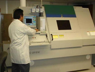
Combination ND: YAG CO2
Forms holes by removing copper with the ND: YAG laser and the dielectric and re-enforcing material with the CO2 laser (Approximately 3,500 to 13,000 holes per minute)
C02 (Infrared)
Capable of drilling most re-enforcing materials and laminate resin systems. Not effective for drilling copper (copper is reflective in the infrared spectrum and must be window etched) Forms holes by pulsing a larger high energy beam (Approximately 17,000 holes per minute)
ND: YAG (Ultra-Violet)
Capable of drilling copper, all re-enforcing materials, and all laminate resin systems. 25 to 50-micron beam forms holes by spiraling or trepanning the beam (Approximately 600 to 1,400 holes per minute).

Combination ND:YAG CO2

ND:YAG (Ultra-Violet)
EMSxchange Enables you to select a Printed Circuit Board, PCB Assembly, cable & wire harness assembly, and box-build suppliers meeting your Required Electronic Manufacturing Capability, capacity, and Certification Criteria from a global Electronic contact manufacturer base.
EMSxchange takes complete responsibility and ownership for your electronic manufacturing process and all its deliverables from contract manufacturing supplier selection to manufacturing to quality inspection to shipment and delivery to your door.
EMSxchange Electronic Manufacturing Partners Profile includes:
Argus Systems (AESPL) – PCB, PCBA, Cable Assembly, Box Build, Testing.