
Test Fixture Probe Tips
Spring loaded test probes are available in a variety of tip styles, plating, spring forces and travel to accommodate any test target.
The test targets can be plated through hole (PTH) leads, plated vias, solder pads, bare vias etc. The internal spring that exerts force on the probe tip is usually selected depending on the surface finish of the test target, higher spring force is required to break through contaminants like oxides, fluxes and other surface preservatives.
High concentration of excessive probe forces can be detrimental around sensitive components which often require Finite Element Analysis (FEA) to determine the correct and safe spring forces and Strain Gage testing for verification of strain levels.
Probe tip selection by surface:
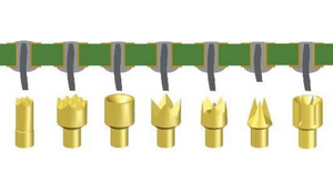
Probe tips for Leads:
Choose the point style which will be most stable on the lead in order to minimize side loading the probe and to extend probe life.
SERRATEDs are generally the most stable on long leads. CUPs can be used on extremely long leads but are likely to require more maintenance.
Standard CROWNs (valleys cut straight across the point) are more stable than self-cleaning styles (valleys sloping down and out).
Point styles with fewer tips or sharper internal geometry such as TRIADs are best used on short contaminated leads. Smaller leads will require tip styles with closely spaced cutting edges to trap the leads.
Probe tip for leads
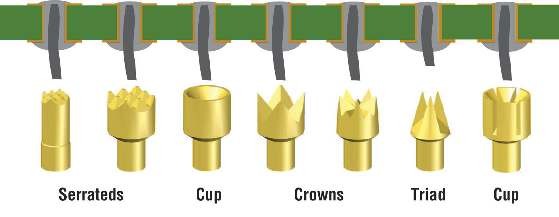
Test Fixture Probe Tips Selection Criteria by surface
SERRATEDs or FLATs are stable on this type of contact, but have little ability to penetrate contamination.
Use FLATs in clean conditions and with higher spring forces. Self-cleaning CROWNs will require less maintenance than CUPs if used in an upward-pointing orientation, but are more likely than a CUP to glance off the post.
Slotted CUPs are best when used upwards, since traditional CUPs can easily collect dust and contamination from the unit under test, they are best used in a horizontal or downward pointing orientation.
Probe tip for terminals and posts
Probe tip for terminals and posts
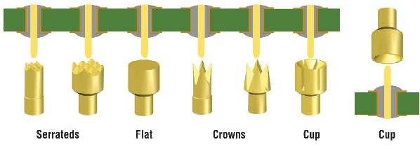
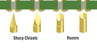
Probe Tips for Pads:
When contacting gold plated pads, CHISEL’s and SPERAS’s are recommended so that marking is minimized.
Reduced CROWNs or TRIADs are good choices for contacting clean flat solder pads, as they distribute the force over a greater area (reducing the likelihood of marking the pad) but require more frequent maintenance.
Use a SPEAR, SHARP CHISEL, SHARP NEEDLE or RAZOR to increase tip contact pressure for reliable testing of heavily oxidized or flux-coated solder pads.

Probe tip for pads
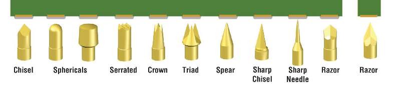
Probe Tips for Holes or Vias:
Use a CHISEL or STAR to contact open holes. CHISELS have fewer contact edges than STARs and therefore higher contact pressure.
The CHISEL TRIAD is a good choice for contacting open holes where flux is present.
The SPEAR is used when the rim of the hole must remain free of marks. Contact is made on a circle rather than on sharp edges.
The BLADEs and RAZORs will provide the highest penetrating pressure since contact is made on just two sharp cutting edges.
Probe tip for holes/vias
Probe tips for Solder Beads / Bumps / Domes:
FLAT tip styles are the least aggressive and are used where minimal witness marks are desired.
The MICRO-SERRATED are more durable and are recommended on points that have light flux residues.
The FLAT STAR is self-cleaning and used when a board will see high cycle counts.
The CENTER POINT STAR is the most aggressive, making them ideal for no-clean flux process where sharper cutting edges are needed.
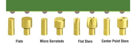
Probe tip for Solder Beads / Bumps / Domes
Required inputs for Test Fixture development Feasibility check
- Number of Test Points Top
- Number of Test Points Bottom
- Test point types
- SMD Test Point Minimum Pad Size (mm)
- SMD Test Point Maximum Pad Size (mm)
- Through Hole Test Point Minimum Hole Size (mm)
- Through Hole Test Point Minimum Hole Size (mm)
- SMD Test Point Minimum TP Pitch to TP pitch (mm)
- Through Hole Test Point Minimum TP Pitch to TP pitch (mm)
- Maximum Hight of the components on Top (mm)
- Maximum Hight of the components on Bottom (mm)
- Board Size (mm x mm)
- How many Number of Boards need to test at a time
- Gerber Files of the device under test
- Minimum Voltage for measuring
- Maximum Voltage for measuring
- Minimum current for measuring
- Maximum current for measuring
- Minimum Frequency for measuring
- Minimum Frequency for measuring
- DUT Board working Voltage
- DUT Board working Current
- Application of DUT Board
EMSxchange Enables you to select a Printed Circuit Board, PCB Assembly, cable & wire harness assembly and box build suppliers meeting your Required Electronic Manufacturing Capability, capacity and Certification Criteria from a global Electronic contact manufacturer base.
EMSxchange takes complete responsibility and ownership for your electronic manufacturing process and all its deliverables from contract manufacturing supplier selection to manufacturing to quality inspection to shipment and delivery to your door. EMSxchange Electronic Manufacturing Partners Profile includes:
Argus Systems (AESPL) – PCB, PCBA, Cable Assembly, Box Build, Testing.
CerraSystems Inc – HDI PCB, Rigid Flex PCB, RF PCB
