
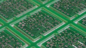
PCB Thermal Management – Metal Coins
- To operate efficiently and ensure reliability, heat must be removed from heat-generating power components. As a result of faster speeds, reduced format, and more devices being populated on PCBs, more heat is being generated that must be removed for efficient operation.
- The move to sustainable energy increased the demand for energy management electronics which also create much heat because of the high electrical currents used in these applications.
- Thermal management through various applications aids in directing heat away from heat-generating system components. The following is a review of various thermal management approaches, applications, and capabilities that can be supported.
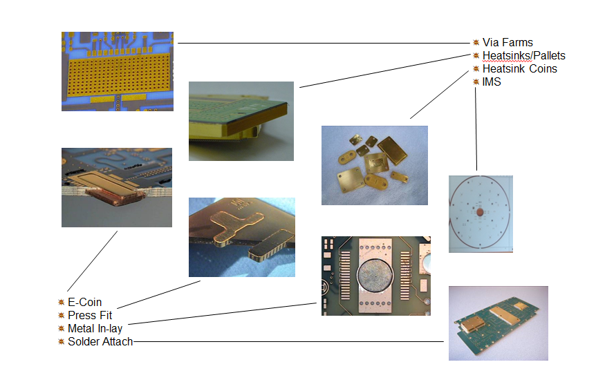
PCB thermal management Options
Embedded Coin
The term Embedded Coin is the general notation for a metal coin that is inserted or contained within a PCB. Variations of Embedded Coins are;
- Copper In-Lay – Circular Press-fit coins
- Press Fit Coins (PFC) where the shape of the coin can be of any configuration typically matching the footprint of the component
- Embedded coins inserted during the lamination process
- E-Coin

Copper In-Lay – Circular Press-fit coins

Press Fit Coins (PFC)
Why choose Embedded Coin-technology over thermal via?
Heat transportation by using Thermal Vias – Rth = 1.3K/W
Heat transportation by using Copper In-lay – Rth = 0.05K/W
As we can see from the result of copper – Inlay process amount of copper makes a significant difference in Heat-spread and ‘Thermal Resistance’ compared to Thermal Via.
Copper In-Lay (Press-fit technology)
- Copper In-Lay (press-fit) is a form of inserting a copper coin or heatsink into a board.
- In this configuration, the coin is round and has small cleats that engage into the opening that was formed during PCB processing.
- The In-Lay / Coin is inserted during the PCB processing.

Copper In-Lay Coin
The Copper In-Lay Coin advantages include below:
- Good thermal dissipation of small devices.
- The In-Lay opening can be tightly controlled (drilling process) resulting in good mechanical retention of the coin.
- Good planarity of the coin surface top and bottom can be maintained
- Lower cost (compared to ‘embedded coin’).
- High volume process (automated assembling) can be supported
Copper In-Lay (Press-fit technology) Process:
Copper in-lay coin Can be supported for Double sided or multi-layer PCB. Typically, the openings are formed by drilling the In-Lay opening. Feature size is more tightly controlled.

Copper in-Lay opening
The In-Lay coins are inserted after the openings have been plated. The retention of the In-Lay is through a mechanical interference fit and final surface finish.

Copper Coin Insertion

Final PCB with copper Coin

PCB with Copper In-Lay Coin

PCB with Copper In-Lay Coin

Copper in-lay Coin Top view

Copper in-lay Coin Cross-section View
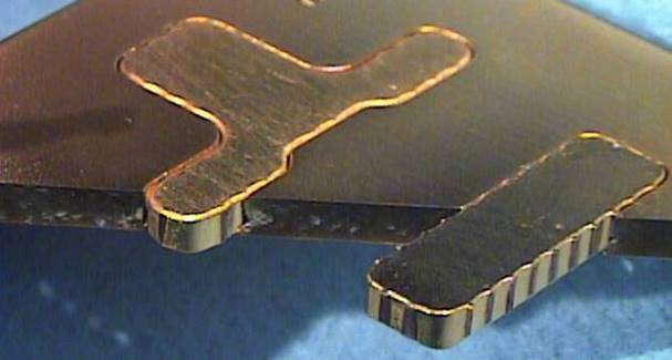
Press Fit Coins (PFC)
Press Fit Coins (PFC) is a derivative of the copper In-lay coin. The primary difference is the heatsink format is typically larger and has a customized shape. The PFC also uses cleats/nubs for coin retention.
- Press Fit Coin’s advantages
- Good thermal dissipation
- Can provide a ground connection through the plated opening to ground layers
- Good planarity of the coin surface top and bottom
- Coin format or size available in almost any format
- More difficult to control the press-fit opening in PCB as the routing process is required
While the Press fit Coin thickness is matched closely to the PCB thickness a primary side should be chosen for the most critical side so that tight planarity of the coin to the PCB surface is desired.
The secondary side may have more variation of planarity due to PCB and coin thickness tolerances.

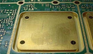
PCB with Press fit coin

Press Fit Coin (PFC) for PCB
Press Fit Coin (PFC) for PCB

Press Fit Coin (PFC) for PCB
Press-fit coin – RF-transistor
- Normally use RO4350B single structure
- Drill countersink
- Press the coin into the cavity
- We need to control the tolerance of cavity size within +/-3mil after plating
- We need to control the tolerance of coin size within +/- 1mil
- We need to control the co-planarity tolerance within +0/- 0.14mm (coin vs. SMT pad around the cavity)
Press-fit coin for RF-transistor
Embedded Coin
The coins in a design are built within the PCB but without the aid of cleats. Straight through all layers (no step, single X & Y dimensions) or Coins can have a step/pedestal design (like E-coin)
Embedded coin advantages;
- May have a ground connection (drilled holes, some thickness restrictions)
- Is bonded to the PCB through prepreg flow of coin openings
- Can be matched for required planarity on the chassis side of the PCB
- Coin format can vary for most application
Embedded Coin PCB Manufacturing Process
Coin opening
Multi-layer PCB is built in sub-part pieces. These sub-assemblies have routed openings to accommodate the coin during the lamination process.

Coin Insertion
Coin is inserted during lamination into the previously created openings in the sub-parts

Embedded Coin
The final PCB with e-coin can now have the heat generating device mounted directly on the coin.

Embedded Coin with co-planer and a recessed top surface

The inserted coin can also be designed such that the surface can be recessed from the top surface. In this case there could be devices that are attached to the coin surface and then attached to the PCB through wire bonding.
Embedded Coin Example

Embedded coin PCB cross-section

Embedded coin PCB cross-section

Embedded coin PCB Top side

Embedded coin PCB Bottom side

Embedded coin PCB Top side

Embedded coin Bottom side
Typical for PCB with high-performance RF transistors coin is recessed from the top surface for component housings that needs to be embedded in PCB and component leads are on the PCB surface.
The RF transistor already is attached to a heat-sink / spreader which is connected to GND and requires a solid connection to the grounded embedded coin in PCB.

E-coin
E-coins uniqueness is the combination of the coin flanges and the application of a thermally and electrically conductive adhesive to aid in grounding contact of the coin to internal ground layers.
The e-coin is inserted into the PCB during the lamination process. The e-coin has several advantages as below
- Good thermal dissipation
- Good electrical grounding
- Good planarity of the coin surface top and bottom
- Reliability of the coin connection due to the encapsulation of the coin by the PCB materials
Multi-layer PCB is built in sub-part pieces. These subs have routed openings to accommodate the coin during final lamination.

Coin opening
The coin is then inserted into the sub-parts during lamination. This completely encapsulates the coin within the PCB structure. The coins were previously prepped with conductive adhesive on the coin flanges.

PCB subassembly with embedded coin
The final PCB with e-coin can now have the heat-generating device mounted directly on the coin. As shown this assembly can then be attached to a secondary heatsink or chassis for additional thermal dissipation.

Final PCB with embedded coin

Embedded Copper Coin
EMSxchange Enables you to select a Printed Circuit Board, PCB Assembly, cable & wire harness assembly, and box-build suppliers meeting your Required Electronic Manufacturing Capability, capacity, and Certification Criteria from a global Electronic contact manufacturer base.
EMSxchange takes complete responsibility and ownership for your electronic manufacturing process and all its deliverables from contract manufacturing supplier selection to manufacturing to quality inspection to shipment and delivery to your door.
EMSxchange Electronic Manufacturing Partners Profile includes:
Argus Systems (AESPL) – PCB, PCBA, Cable Assembly, Box Build, Testing.
