
PCB Reverse engineering is critical for determining functionality, forensic analysis, intelligence, or testing/verifying. With Reverse Engineering one can clone the design (e.g., to recreate a previous design whose documentation has been lost , identify areas where new features/capabilities can be added, locate specific connections, or derive how a product works by creating a schematic diagram.
PCB Reverse engineering process requires to access and image each layer of the target circuit board. When all layers are placed together, a complete circuit layout is identified.
This Article provides details on PCB deconstruction, including solder mask removal, delayering, and imaging, and provided a number of practical, effective techniques that could be used to access individual layers of a target Printed circuit board.
1. PCB Composition
PCBs are created with layers of thin conductive copper foil laminated to non‐conductive insulating layers. They form the physical carrier and provide electrical pathways between electronic components.
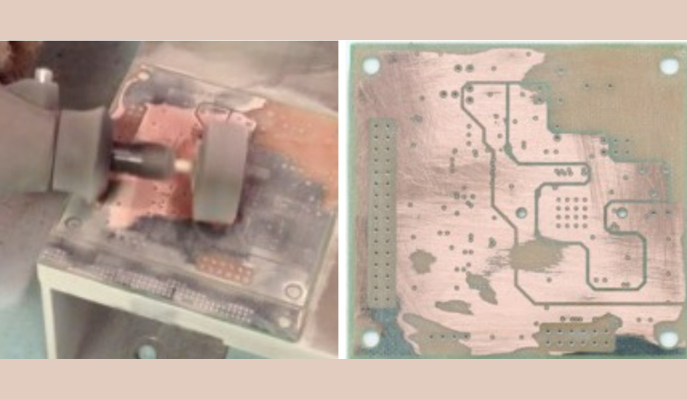
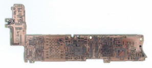
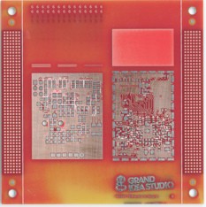
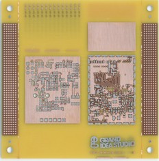
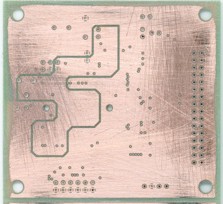
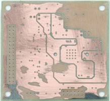
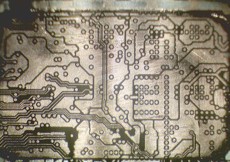
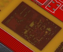
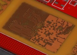
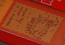
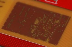
By accessing and imaging each individual copper layer of a PCB (Fig. 1), it is possible to reverse engineer the entire PCB layout.
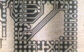
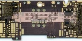
State‐of‐the‐art PCB manufacturing processes support trace and space widths less than 1mil, laser‐drilled microvia diameters of 0.4mil, via-in-pad construction, and passive electronic components embedded into substrate. Copper thickness typically ranges from 0.5oz to 4oz . A PCB cross-section provides clues to its design and complexity (Fig. 2).
Once a PCB is fabricated, its surface is coated with solder mask (solder resist). Comprised of epoxy, liquid photo imageable ink (LPI), or dry film photo imageable material, this non‐conductive layer protects the PCB Reverse engineering from dust and oxidation, and provides access to copper areas on the board that are desired to be exposed (such as component pads or test points).
A thin surface finish, in the form of lead‐based or lead-free solder, tin, silver, gold, or palladium, is then applied to the exposed copper to enhance solderability and/or for harder contact surfaces.
Finally, silk- screen is printed onto the board using epoxy or printable ink. This layer often contains the part designators, identification symbols, logos, and other manufacturing markings.
2. Solder Mask Removal
The goal of this phase is to remove the solder mask from the PCB and expose the copper traces on the top and/or bottom layers with minimal damage. While it’s sometimes possible to identify the copper traces through existing solder mask, removing the solder mask will give a clearer view. The following Solder mask removal processes assume there are no components are populated on the target PCB ( Bare PCB )
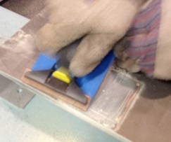
2.1 Sandpaper – Solder Mask Removal
Sandpaper is an effective and low-cost method for solder mask removal. We can obtain the best results by clamping the target PCB to a work table and using the sandpaper, held by hand, in even strokes at light pressure across the entire PCB surface (Fig. 3).
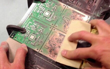
Spare PCBs of the same height and thickness as the target PCB Reverse engineering should be used as support material on both sides to help maintain planar motion and even sanding pressure. Care must be taken to ensure that the underlying copper layer isn’t damaged by excessive abrasion.
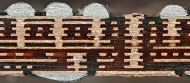
Different PCB surface finishes require different sandpaper grit sizes. For example, on a PCB with thick hot air solder leveling (HASL) finish, first use 60 grit sandpaper to remove the thick solder from all of the exposed copper pads and then used 220 grit sandpaper to complete the solder mask removal.
On the PCB Reverse engineering which has immersion gold plating, thinner solder mask, and trace/space less than 3/3mil, use a less abrasive 400 grit sandpaper (Fig. 4).
2.2 Fiberglass Scratch Brush – Solder Mask Removal
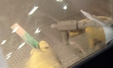
Fiberglass scratch brushes are handheld, pencil-shaped tools used for material cleaning and polishing. For example, use an Excelta fiberglass scratch brush in even strokes at medium pressure (Fig. 5).
2.3 Abrasive Blasting – Solder Mask Removal
Abrasive blasting is a method of forcibly propelling a stream of abrasive material against a target object to strip material from surfaces (e.g., from paint, calcium deposits, or fungus) or add texture/ artificial wear to a product. The abrasive material comes in many forms to suit different materials and finishes, including garnet, glass beads, crushed walnut shells, and synthetic abrasives.
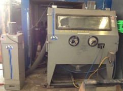
For example, use Abrasive Blasting cabinet ( SkatBlast ) with an 80 PSI, 10-15 cubic feet per minute (CFM) output of 60 grit aluminum oxide (Fig. 6). Best results are obtained when the nozzle Is angled and held 6” to 8” away from the PCB.
The copper and underlying substrate remains intact, though there might be pitting due to the abrasive media (Fig. 7).
Abrasive blasting is most suited for PCBs with large features (10/10mil trace/space or greater) and copper weight of 1oz (1.4mil) or more. Regardless of PCB construction, there is a risk of damaging underlying copper by use of abrasive blaster on one area of the PCB for too long.
2.4 Chemical – Solder Mask Removal
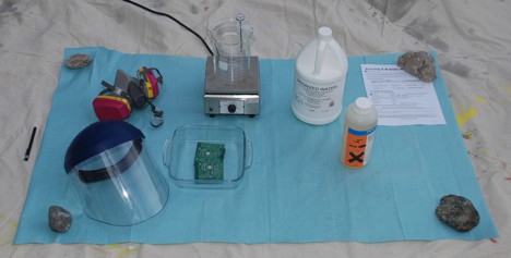
There are chemicals specifically formulated for purpose of removing solder mask (For example Ristoff C-8 and MagnaStrip 500). The Typical workspace for chemical process consists of a chemical-resistant drop cloth, hot plate, beaker, thermometer, glass tray, stainless steel tongs, and safety equipment (Fig. 8).
Ristoff C-8, works against fully cured, aqueous developable LPI and ultraviolet (UV) curable solder masks. The chemical comes in a concentrated form and requires a 50/50 mix with deionized water before use.
Magnastrip 500, works against fully cured, LPI acrylic solder masks, but does not work against screen printed epoxy thermal-cured solder masks. The chemical comes ready-to-use and does not require any dilution.
Both chemicals have similar recommended operating procedures as below
- Heat the chemical to 120-140°F (up to 200°F for Magnastrip 500).
- Place the target PCB Reverse engineering into the beaker and wait for solder mask stripping to occur (45-120 minutes for Ristoff C-8 and 15-60 minutes for Magnastrip 500). Actual processing time will vary due to chemical temperature, solder mask composition, and solder mask thickness. As the solder mask brakes down, it flakes off the PCB into the solution.
- Remove the PCB from the beaker and brushed lightly with a soft metal brush under running water. This helps to lift any remaining solder mask from the board.
The results for both chemicals produce clean, exposed top/bottom copper layers with no abrasion or scratching (Fig. 9 and 10).
2.5 Laser – Solder Mask Removal
Laser skiving is traditionally used for selective, highly controlled material removal or rework (e.g., accessing and/or cutting a single trace on a PCB’s inner layer).
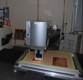
For example use a LPKF Micro- Line 600D UV Laser System (Fig. 11), which is de- signed for accurate (+/-0.6mil), stress free cutting of flex circuits and coverlayer material (e.g., foil, film, or adhesive).
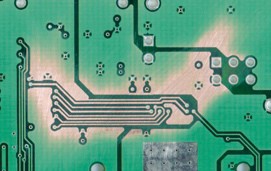
Run single passes at medium power across small, specific areas of target PCBs. The laser successfully removes solder mask leaving copper fully intact (Fig. 12). The carbon residue/soot remaining on the exposed copper surfaces should be removed with steel wool under running water.
Solder mask and substrate react more quickly to the UV laser than copper, so care must be taken to ensure that the laser power is properly adjusted to the minimum required for a given target PCB Reverse engineering. Otherwise, subsequent copper layers could be exposed as inner layer substrates are inadvertently removed.
With the laser traveling at a maximum speed of 300mm/second and a beam diameter of approximately 20um processing an entire PCB could take anywhere from a few minutes to a few hours depending on surface area and solder mask thickness.
3. Delayering
The goal of this phase is to access the inner copper layers of a multi-layer PCB by way of physical, destructive delayering. The following processes assume no components are populated on the target PCB.
3.1 Sandpaper – PCB Delayering
Sandpaper is an effective and low-cost method for removing layers of PCB material. Mount the target PCB to work table with double-sided tape and Then, use 60 grit sandpaper held by a Sheet Sander tool in hard, full strokes across the entire PCB area (Fig. 13).
The resulting layer might exhibit minor scratching and noticeable wearing of copper along the edges due to uneven sanding.
3.2 Dremel Sander – PCB Delayering
The Dremel flap wheel sander is a common tool used in a variety of applications, including grinding, polishing, and sanding and can be used to expose layer 3 of the target PCB Reverse engineering using back and forth motions at medium pressure. ( (Fig. 14)
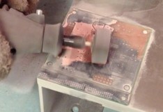
The flap wheel (120 grit, 3/8” wide) must be kept flat in order to prevent an edge from digging into the PCB. Also, a flexible shaft might be used to help move the body of the tool away from the work surface and make it easier to keep the flap wheel flat against the PCB.
3.3 CNC Milling – PCB Delayering
CNC milling machines are used for highly accurate, computer-controlled removal or engraving of material. Many different types of CNC milling equipment exist, including PCB prototyping machines, which create custom PCBs by milling traces and pads on copper-clad stock.
For example, use QuickCircuit 5000 (Fig. 15) with a 1/8” diameter carbide endmill specifically designed for working with non- ferrous materials. Control and manipulation of milling, drilling, and routing procedures are achieved including tool type, tool cutting depth Z-axis (can be adjusted in 10um (0.4mil) increments.) and solenoid force selection
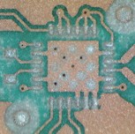
In order to access the inner layers First, a mechanical outline of the desired PCB area is created and configured to rubout all material inside of the area (Fig. 16).
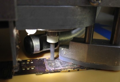
This step provided accurate, repeatable, and automatic positioning of the milling path, as opposed to manually controlling the machine. Then, adjust the Z-axis depth in approximately 1mil increments between runs of the milling machine (set to move at a rate of 8”/minute with a spindle speed of 24,000 RPM). When we begin to see the next layer of copper beneath the substrate, stop milling and use a fiberglass scratch brush to remove the remaining substrate and expose the area.
The method requires time and patience to slowly increase the Z-axis depth to avoid accidental damage of the target PCB’s inner layers.
3.4 Surface Grinding – PCB Delayering
Surface grinding is an abrasive machining process used for material grinding and surface finishing. A surface grinding machine consists of a rotating abrasive wheel (also known as a grinding wheel), work surface, and a
reciprocating or rotary table controlled manually or by a computer.
For example, use a CNC Creep Feed Surface Grinder (PROFIMAT) with a 1 3/8”-wide grinding wheel (Fig. 18). Machine is highly precise and allows depth control in 0.1mil increments. Machine should be properly aligned to the target material and configured to the desired grinding parameters and surface
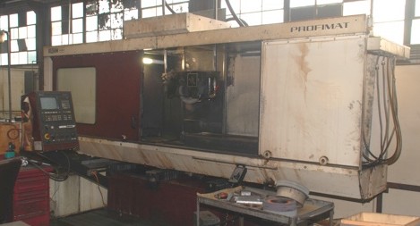
Target PCB Reverse engineering is mounted to a 1” steel block, which is held in place by the machine’s magnetic chuck. The depth is adjusted in small increments (starting at 0.5mil and increasing to 2mil) in between runs of the surface grinder until we were able to see the next layer of copper beneath the substrate.
If the target PCB’s inter-layer spacing is known or can be determined with a cross-section measurement, less trial and error will be necessary and the process can be expedited.
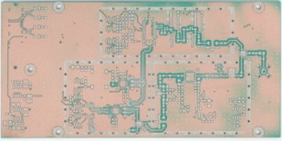
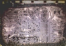
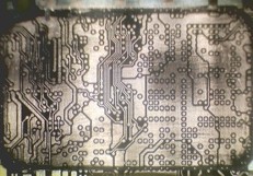
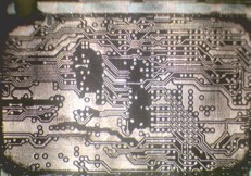
With Surface grinding process (Fig. 19) each copper layer is clearly visible through the remaining fiberglass substrate. This precludes the need to fully expose the copper layer in order to obtain a usable image.
Grinding process works well with PCBs of nearly any size, though custom mounting methods may need to be created for boards that do not contain mounting holes or to help flatten a board that is bowing/flexing.
Ensure that during Grinding process Target PCB is not removed from the machine part way through the process, as properly realigning the PCB is difficult and may affect subsequent grinding runs.
4. PCB Reverse Engineering with Imaging
The goal of this phase is to obtain individual image layers of a multi-layer PCB using non-destructive imaging techniques.
4.1 X-ray (2D)
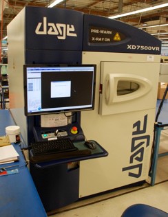
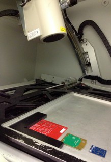
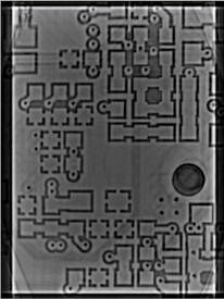
X-ray inspection equipment is typically used during the PCB assembly process to verify component placement and proper solder quality, or after the assembly process for failure analysis to identify, locate, or troubleshoot defective features. X-ray waves are emitted from an X- ray tube on one side of the target object and captured by a detector on the opposite side. (Fig. 20)
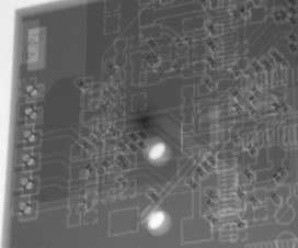
For each PCB, a series of X-ray images are taken at a variety of angles and contrasts. Due to the nature of 2D X-ray imaging, the resulting images are composites of all PCB layers. For multilayer Boards it makes it difficult to determine on which layer a particular trace is located (Fig. 21).
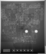
With 2D X-ray inspection we can get a general sense of PCB construction/ layout and, for simple boards, visually follow traces/ connections by manipulating the X-ray’s angle and field-of-view in real time. However, it is time consuming and tedious process to recreate full image layers using this method.
4.2 Computerized Tomography (3D X- ray)
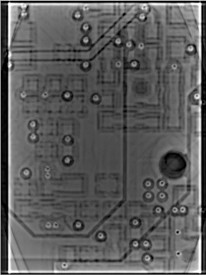
Computerized Tomography (CT) is an X-ray imaging method where a series of 2D X-ray images are post- processed to create cross-sectional slices of the target object. CT is frequently employed for complex inspection and failure analysis of PCBs, electronic component packaging, and solder ball quality.
First step is to capture a series of 2D X-ray images (depending on the desired resolution of the resulting cross-sectional slices) by rotating the X-ray 360° in a single axis around the target object (Typically 50° inclination angle), after mathematical post-processing of the 2D slices of images could be viewed in any plane (X, Y, or Z).
These images slices are then imported into an off-the-shelf software tool used for 3D model manipulation (VGStudio,), which provides a graphical environment to more easily analyze the images and to add various effects to show depth or highlight specific areas (Fig. 22).
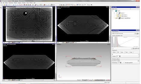
We can move through the slices along the Z plane (from top to bottom through the PCB) and easily identify each of the target PCB’s layers (Fig. 23). Note that the success of CT may vary depending on PCB construction features, such as layer stack-up, material composition, copper weight, and component placement.
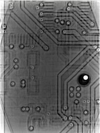
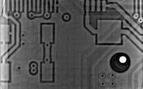
Limitation of CT is the size of the X-ray system’s field-of-view. The more area that is visible within the field-of-view, the less resolution/detail will exist on the acquired images. We need to find the balance between sufficient board visibility and image quality, which in most cases won’t comprise the entire PCB area. In order to process a full PCB, multiple “segments” are created and stitched together.
5. Characterization matrix of PCB deconstruction techniques
Below table provides a list of PCB deconstruction techniques along with a characterization of each based on the time re- quired, cost, access to equipment, ease of use, likely-hood of success, and quality of result. These criteria can be used to aid in the selection of the most appropriate method for a particular situation.
| Technique | Time Required | Cost | Access to Equipment | Ease of Use | Likelihood of Success | Quality of Result |
| Solder Mask Removal | ||||||
| Sandpaper | <1 hour | low | Easy | Easy | Fair | Good |
| Fiberglass scratch brush | <1 hour | low | Easy | Easy | Excellent | Excellent |
| Abrasive sand blasting | <1 hour | Mid | Moderate | Medium | Fair | Good |
| Chemical | 4 hours | Mid | Difficult | Hard | Excellent | Excellent |
| Laser | 4 hours | High | Moderate | Hard | Varies | Excellent |
| Delayering | ||||||
| Sandpaper | 4 hours | Low | Easy | Easy | Fair | Excellent |
| Dremel tool | <1 hour | Low | Easy | Medium | Poor | Varies |
| CNC milling | 4 hours | Mid | Moderate | Hard | Excellent | Excellent |
| Surface grinding | 4 hours | High | Moderate | Hard | Excellent | Excellent |
| Imaging | ||||||
| X-ray | 8+ Hours | High | Moderate | Medium | Poor | Varies |
| CT X-ray | 2 hours | High | Moderate | Medium | Fair | Excellent |
EMSxchange Enables you to select a Printed Circuit Board assembly, cable & wire harness assembly and box build suppliers meeting your Required PCBA Manufacturing Capability, capacity and Certification Criteria from a global PCB Assembly manufacturer base.
EMSXchange takes complete responsibility and ownership for your electronic manufacturing process and all its deliverables from contract manufacturing supplier selection to manufacturing to quality inspection to shipment and delivery to your door. EMSxchange Electronic Manufacturing Partners Profile includes:
Argus Sytems (AESPL) – PCBA, Cable Assembly, Box Build.
Cerra Systems inc – PCB Manufacturing.