
Definition of Reliability
- Reliability is the ability of an apparatus, machine, or system to consistently perform its intended or required function or mission, on-demand and without degradation or failure.
Military standard definition of reliability
- Reliability is the probability that an item will perform a required function without failure under stated conditions for a stated period of time.
Examples of High-Reliability Applications

Drones – IPC Class 3 – High Reliability

Oil Wells – Extreme High-Reliability PCB
Institute for Interconnecting and Packaging Electronic Circuits (IPC) Develops and distributes standards to PCB designers, users, suppliers, and fabricators
- Class 1
- Consumer products, including TV sets, toys, entertainment electronics, and non-critical consumer or industrial control devices
- Class 2
- General industrial, including computers, telecom equipment, business machines, and non-critical military applications
- Class 3
- High reliability, including equipment where continued performance is critical, life support & Military
- Class 3A
- Performance Specification for Space & Military
IPC 6011/6012 Classification
- Type 1
- Single–Sided
- Type 2
- Double-Sided
- Type 3
- Multilayer without blind & buried vias
- High Reliability
- Type 4
- Multilayer with blind & buried vias
- High-Reliability Advanced
- Type 5
- Copper core Multilayer without blind & buried vias
- Type 6
- Copper core Multilayer with blind & buried vias
MIL-PRF-55110G – Military Performance Specification
- Type 1
- Single–Sided
- Type 2
- Double-Sided
- Type 3 – High-Reliability Advanced
- Multilayer includes metal core and blind & buried vias
MIL-PRF-31032/5 – Military Performance Specification
- Type 1
- Single–Sided
- Type 2
- Double-Sided
- Type 3 – High Reliability
- Rigid Multilayer without blind or buried vias
- Type 4 – High-Reliability Advanced
- Rigid Multilayer with blind & buried vias
- Type 5
- Rigid Multilayer without blind or buried vias with metal core or metal backing external heat-sink
- Type 6
- Rigid Multilayer with blind or buried vias with metal core or metal backing external heat-sink
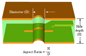
Aspect Ratio: Through Holes and Microvias
- Aspect Ratio Drives the Drill Diameter (10:1 Standard)
- Increasing layer counts and reduced hole diameters are driving Aspect Ratios beyond the limits of standard electroplating
- High Aspect Ratio requires Complex Waveform Pulse Plating
- Copper deposition is enhanced By modifying the plating chemistry In the reverse current cycle to Reduce copper deposition in high Current density areas of the hole Barrel, resulting in uniform plating
Mechanically drilled through hole Via
Mechanically drilled through hole that will be used to penetrate the entire thickness of the PCB or a through hole that will be used in a mechanically drilled sub-lamination used to form blind or buried vias.
In this configuration, the depth of the hole is measured from the surface of the external copper layers. In this case, if the hole diameter was 0.010” and the depth was 0.093” the Aspect Ratio would be 9.3 to 1
Mechanically drilled through hole Via
Laser drilled micro vias
Laser-drilled micro vias are controlled depth hole that terminates on a copper layer. As a result, the depth of the hole is calculated from the top of the terminating layer to the top of the copper foil layer on the hole entrance. In this case, if the hole diameter was 0.006” and the depth was 0.003” the Aspect Ratio would be 0.5 to 1.
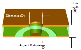
Laser drilled micro vias
Design rules for Microvia build-up layers
- Build-up dielectric layers must be balanced on either side of the sub-lamination
- Build-up dielectric layers are generally 0.0025” to 0.003” thick
- The recommended total number of lamination cycles that any one part of the structure should experience is 3 and 4 – 5 for advanced structures
- Microvias stacked on buried mechanical vias should be avoided due to wrap plating requirements and excessive stress on thicker substrates
- Solid copper mechanically drilled via’s can be used on thin sub-lamination cores in place of wrap plating
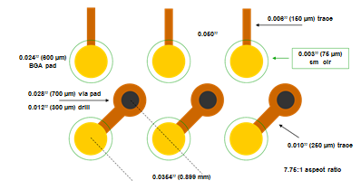
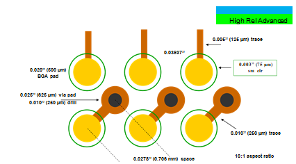
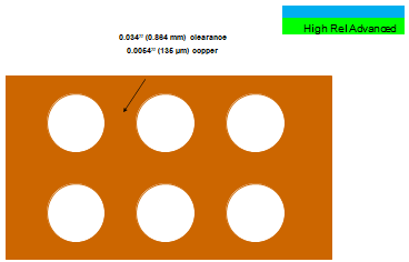
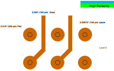
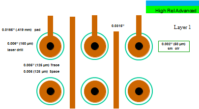
BGA Design Guidelines for High Reliability PCB
1.27 mm BGA – IPC 6012 Class 3 – External Layer
1.27 mm BGA – IPC 6012 Class 3 – Internal Layer
1.27 mm BGA – IPC 6012 Class 3 – Internal Layer
1.27 mm BGA – IPC 6012 Class 3
0.035” (0.889 mm) clearance

1 mm BGA – IPC 6012 Class 3 – External Layer
1.27 mm BGA – IPC 6012 Class 3 – Internal Layer
1 mm BGA – IPC 6012 Class 3 – Internal Layer
0.8 mm BGA – Microvia Technology
0.8 mm BGA – Microvia Via-in-Pad Technology
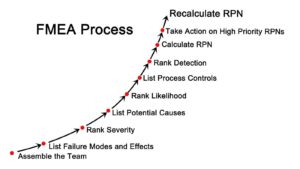
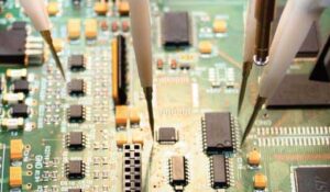
PCB Integrity and Reliability Evaluation
- Interconnect Stress Test (IST)
Interconnect Stress Test (IST) is an accelerated stress test method used to evaluate the integrity of the Printed Circuit Board (PCB) interconnect structure.
- Highly Accelerated Thermal Shock (HATS)
The HATS system’s programmable self-contained machine will do all the common reliability cycles, with a range from -55°C to +145°C in air-to-air mode.
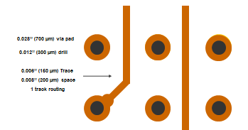
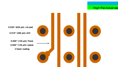
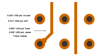
PCB Design Considerations for high reliability PCB
- The key to a successful Design is the right combination of trace width & space, drill diameter, pad diameter, anti-pad, and aspect ratio. This will maximize routing density, improve electrical characteristics, and allows the PCB to be fabricated with high yields for the lowest cost in a timely manner.
- Maintain robust Trace & Space (0.005” trace & space)
- 10:1 aspect ratio or lower
- Min of 0.0012” copper on the wall of plated holes (Class 3A avg 0.0015”)
- Single lamination cycle (symmetrical construction – copper – laminate – prepreg)
- Utilize Solid Copper Microvias if required (Via-in-Pad OK)
- Maintain 70% copper density or greater (add copper pour if needed)
- Eliminate through-hole via-in-Pad with non-conductive fill and plate
- Choose the Right PCB Material for your application
- Impedance Tolerance 10%
- IST & HATS Test to determine relative long-term reliability
- Keep it Simple (Different Levels for High-Reliability Design)
EMSxchange Enables you to select a Printed Circuit Board, PCB Assembly, cable & wire harness assembly, and box-build suppliers meeting your Required Electronic Manufacturing Capability, capacity, and Certification Criteria from a global Electronic contact manufacturer base.
EMSxchange takes complete responsibility and ownership for your electronic manufacturing process and all its deliverables from contract manufacturing supplier selection to manufacturing to quality inspection to shipment and delivery to your door.
EMSxchange Electronic Manufacturing Partners Profile includes:
Argus Systems (AESPL) – PCB, PCBA, Cable Assembly, Box Build, Testing.