
What is considered a Microvia?
- Laser Drilled Blind Via from the outer layer to an inner layer
- 150 µm (0.006”) diameter laser drill (range 100 µm (0.004”) – 200 µm (0.008”)
- Laser drill directly into BGA or SMT footprint (Via-in-Pad)
- Eliminate through-hole vias
- Increases routing density & enhances electrical characteristics
- Maintain a 0.5:1 aspect ratio or advanced 0.8:1
- Provides fan-out solutions
- Microvias terminate to the underlying pad without penetrating the copper
Microvia Types
- Standard – Single Lamination cycle (no Buried Via)
- Standard – with buried via
- Staggered or stair-step
- Off-set Microvias
- Stacked Microvias are required for 0.4 mm pitch
- Deep Microvias
Standard Microvias create routing density (eliminate through vias)
- Reduce layer count
- Enhance electrical characteristics
- Standard Microvias are limited to layers 1 – 2 & 1 – 3
Stacked Microvias allow increased routing on multiple layers
- Provide Solutions for next-generation applications such as 1 mm – 0.8 mm – 0.65 mm – 0.5 mm – 0.4 mm – 0.3 mm & 0.25 mm
- SMV provides a solid copper plate eliminating potential solder voiding
Deep Microvias
- Provides additional dielectric material & small geometry features, improved Impedance performance & provides RF Microvia solutions
Deep Stacked Microvias
- Provides additional dielectric while maintaining small geometries on multiple layers
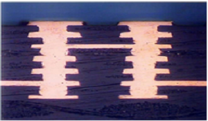
Single Microvia
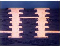
Stacked Microvias
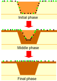
Electroplated Copper via filling Mechanism
- Bottom-up filling behavior is attributed to the action of organic additives (must be controlled to prescribed limits)
- Suppressor rapidly forms a current inhibiting film on the Cu surface. The film has little geometric dependence due to the high suppressor solution concentration
- Accelerated bottom-up fill behavior is due to a local accumulation of brightener species at the feature base
- As surface area is reduced during deposition, the concentration of brightener species increases, resulting in a non-equilibrium surface concentration. This local concentration of brightener accelerates the plating rate relative to the surface.
- Brightener
Electroplated Copper via filling Mechanism

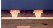
Planar Microvia
Stacked Microvia
Copper Via filling Advantages:
- Design flexibility (SMV post or buried SMV) single or stacked
- Provides a solid copper plate
- Improves Current Carrying Capability & Thermal Management
- Provides a Planar surface for BGA (Via-in-Pad)
- Increases routing density for Fine Pitch BGAs (0.65 mm, 0.5 mm, 0.4 mm, 0.3 mm& 0.25 mm)
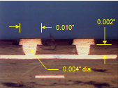
- Allows Design Fan-out on multiple layers using 0.010” (250 µm), 0.008” (200 µm), and 0.007” (175 µm) pad diameters
Design Guidelines:
Pad diameters are driven by device pitch, and drill diameter is driven by the dielectric thickness
- First consideration for via hole diameter is aspect ratio and reliability
- Regardless of the hole via-hole diameter IPC Class III requires a larger minimum pad diameter than IPC Class II
- When designing to class II with minimum pad diameters it is important to maintain a minimum of 8 mils from the primary drill hole edge to any copper features.
- Signal routing channels come in integer values (i.e. 1,2,3…. n)
- Signal track width should be selected based on the electrical requirements
- Track width and pad diameter should be maximized to take advantage of via pitch with respect to the maximum integer value of signal routes (in other words, don’t shrink pads and or track widths if it does not create another signal route!)
Standard
- 0.012” (300 µm) Pad diameter & 0.006” (150 µm) laser drill
- 0.5:1 aspect ratio
- 0.010” (250 µm) Pad diameter & 0.005” (125 µm) laser drill
Advanced
- 0.0086” (218 µm) Pad diameter & 0.005” (125 µm) laser drill
Flip Chip Solution
- 0.007” (175 µm) Pad diameter & 0.004” (100 µm) laser drill
EMSxchange Enables you to select a Printed Circuit Board, PCB Assembly, cable & wire harness assembly, and box-build suppliers meeting your Required Electronic Manufacturing Capability, capacity, and Certification Criteria from a global Electronic contact manufacturer base.
EMSxchange takes complete responsibility and ownership for your electronic manufacturing process and all its deliverables from contract manufacturing supplier selection to manufacturing to quality inspection to shipment and delivery to your door.
EMSxchange Electronic Manufacturing Partners Profile includes:
Argus Systems (AESPL) – PCB, PCBA, Cable Assembly, Box Build, Testing.