
Soldering Methods for PCB Assembly
How should an engineer go about adopting the right soldering method?
This is probably a question that most electronics engineers face. The first thing that needs to be done is selecting the soldering method best suited to an application by considering the pros and cons of each soldering method, as well as the heat resistance of the surface-mount device.
Soldering methods are broadly divided into the partial-heating method and the total-heating method. While heat is applied to the components’ leads and printed wiring boards (PWBs) in a localized manner in the partial-heating method, in the total-heating method sees, heat is applied to the entire board. This means that partial heating involves less heat stress on the device and PCB, but is unsuitable for large-volume production. Therefore, this method is mainly used to correct soldering or for devices with low heat resistance.
The total-heating method is excellent in terms of productivity and running cost, but it can place considerable heat stress on the semiconductor device and board. In both cases, engineers should learn to validate the process with respect to the job they intend to carry out.
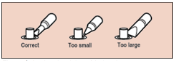
Fig. 1: Selecting the right soldering tip
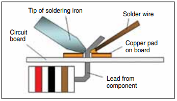
Fig. 2: Correct positioning of the solder tip
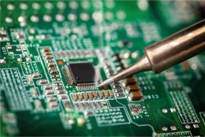
Partial-heating method: Hand soldering
Selecting the right soldering tip and iron
This is something that needs to be practically validated according to the nature of the job and the components used. The job dimension and tip dimension, which is about 0.5mm to 5.0mm wide, with different types of shapes like C type (round chamber shape) or D type (flat screwdriver type), need to be selected. The proximity of other components also needs to be considered. See Fig. 1 for clarity.
Thermal effects
Controlling the soldering iron tip temperature using the controls available on the soldering equipment is not the key element in soldering. The key element is in controlling the heat cycle of the work in terms of how fast it gets hot, how hot it gets, and how long it stays hot for reliable solder connections.
Engineers should also learn about process validation of the soldering process with respect to job dimension, tip dimension, solder-wire dimension, and temperature. Based on validation results and the operator’s speed of performing soldering, the temperature should be set between the minimum and maximum range of validated temperature for a particular job.
Maintaining the soldering tips
The optimum temperature at which proper soldering takes place should be set so that overheating is avoided. When the tip is cleaned on the sponge, the sponge should have only moisture; water should not drop from the sponge while squeezing it and you should only feel the moistness. Hence, it should be moistened to that level periodically.
Solder tips should not be rubbed or sharpened with a hard surface nor should these be tapped on the table. The handle set must always be kept with the tip in the stand when not in use, preferably with the tip covered in solder. Almost every day the tip should be removed from the in-place element, followed by cleaning the element with a dry soft cloth and refitting the tip.
Reducing the occurrence of solder balls and other defects
The hot solder tip should not touch the solder wire while soldering a joint. The solder wire should be kept on one side of the job and the tip on the other side or on a different location on the job but as close as possible. This should be practiced in order to avoid the occurrence of solder balls.
Precautions
Some components, such as transistors, can get damaged by heat when soldering. It is wise to use a heat sink clipped to the lead between the joint and component body, as shown in Fig. 3. You can buy a special tool, but a standard crocodile clip works just as well and is cheaper!
Ensuring reliable solder connections.
Reliable solder connections can only be accomplished with truly cleaned surfaces of copper pads and component leads. But usually, the pads and component leads may be contaminated due to the film of the oxide layer formed over their surfaces. This could cause poor soldering. Hence, before performing a soldering process, one needs to ensure the cleanliness of the surfaces. For this purpose, fluxes are used.
These consist of natural or synthetic resins as well as chemical additives called activators. It is the function of these fluxes to remove oxides and keep these removed during the soldering operation. This is accomplished by the flux action, which is very corrosive at solder-melt temperatures and accounts for the flux’s ability to rapidly remove metal oxides.
In its unheated state, however, rosin flux is non-corrosive and nonconductive and thus will not affect the circuitry. It is the fluxing action of removing oxides and carrying these away as well as preventing the reformation of new oxides that allows the solder to form the desired intermetallic bond.
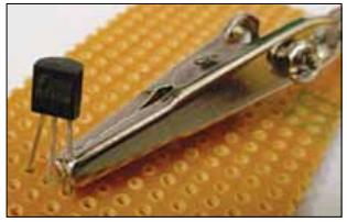
Fig. 3: A crocodile clip holding the heat sink in place
Total-heating method: Wave soldering and SMT reflow soldering
Parameters for validation.
In this process, parameters to be considered for validation are pre-heating temperature, flux (clean or no-clean flux as appropriate) level and its level of foam generation, solder combination of tin (SN) and lead (PB), solder level, its temperature and level of wave generation. Last, but not least, is conveyer speed.
Pre-heating is required to avoid thermal shock and get better cleaning during flux contact, which, in turn, gets better solder ability. Optimum levels of flux contacts help avoid the formation of solder balls and allow for better solder ability with proper wetting.
In the reflow soldering process, parameters to be considered for validation are the size of the pad and the selection of solder paste grain sizes. For instance, a smaller-size pad will require an appropriate amount of solder paste having solder powder with smaller particle diameters. Other parameters include temperature profiling throughout the reflow oven at different stages and the speed of the conveyor.
Profile stages of an SMT reflow process
The four profile stages of an SMT reflow process are pre-heat, pre-reflow, reflow, and cooling.
Pre-heat– This phase conditions the PCB assembly before the actual reflow takes place on the pad. It removes dirt and oxides by the volatile flux action (the flux compound present in the solder paste itself depends on the selected solder paste) and reduces thermal shock to the PCB assembly.
Pre-reflow- In this phase, surfaces (the pad and components) are prepared to get joined by the removal of dirt or oxide layers and other impurities present in the solder paste.
Reflow – This is where the actual reflow of the solder alloy creates the mechanical and electrical bond through the formation of solder (tin-lead) and copper inter-metallic bonding.
Cooling –This phase is important because the formation of the grain structure of the solder joint happens now. Most reliable solder joints are achieved by the appropriate cooling rate set by proper validation results.
Reducing the possibility of defects
When validations are ineffective, these give rise to pin holes or blow holes, poor wetting, cracks, and less or excess solder, among other issues related to soldering. Other defects are a component failure due to high soldering temperature or sustained heat transfer due to low conveyor speed. However, a good visual inspection and touch-up by hand soldering can avoid residual defects after setting up a properly validated process.
Possible defects in the reflow soldering process include voids due to poor cleaning action on the pad surface and grappling, which is a phenomenon that appears as poor reflow of solder particles at the top of the solder. Smaller components are also susceptible to tomb-stoning, wherein components get lifted from the pad with uneven solder paste filled underneath.
Higher temperatures and long sustenance of heat make components susceptible to component failure. This may be immediate or latent.
EMSxchange Enables you to select a Printed Circuit Board, PCB Assembly, cable & wire harness assembly, and box-build suppliers meeting your Required Electronic Manufacturing Capability, capacity, and Certification Criteria from a global Electronic contact manufacturer base.
EMSxchange takes complete responsibility and ownership for your electronic manufacturing process and all its deliverables from contract manufacturing supplier selection to manufacturing to quality inspection to shipment and delivery to your door.
EMSxchange Electronic Manufacturing Partners Profile includes:
Argus Systems (AESPL) – PCB, PCBA, Cable Assembly, Box Build, Testing.
CerraSystems Inc – HDI PCB, Rigid Flex PCB, RF PCB