
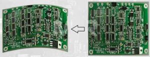
PCB Assembly Warpage
- The substrate (copper clad) may be one of the causes of PCB Assembly Warpage, but thermal stress, chemical impacts, and faulty production techniques can also cause printing during the processing of printed circuit boards.
- It is an unintended change in the geometry of a PCB. The reasons can be either PCB layout or assembly process related.
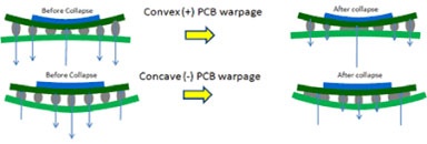
- PCB warpage Results in a concave or convex PCB shape.
How it Occurs?
- Warping of flat or planar PCB is a significant yet common problem when manufacturing and assembling PCBs.
- The factors which contribute to warping includes below
- Balance between the circuit area and the conductor pattern (Copper layer distribution).
- Symmetry of the circuit board stacking.
- Irregular/Odd shape of PCB.
- Conveyor setup at PCB FAB & Assembly process stage.
- Presence of Moisture .
- Operating Temperature.
How it Affect the Quality
- For surface mount technology, the IPC-6012 standard defines the maximum bow and twist or warping to 0.75%. However, for Rigid PCBs with thicknesses of around 1.6 mm and using fine pitch SMDs and BGAs can only stand warping to the extent of 0.5%
- Impact of warpage effects Includes:
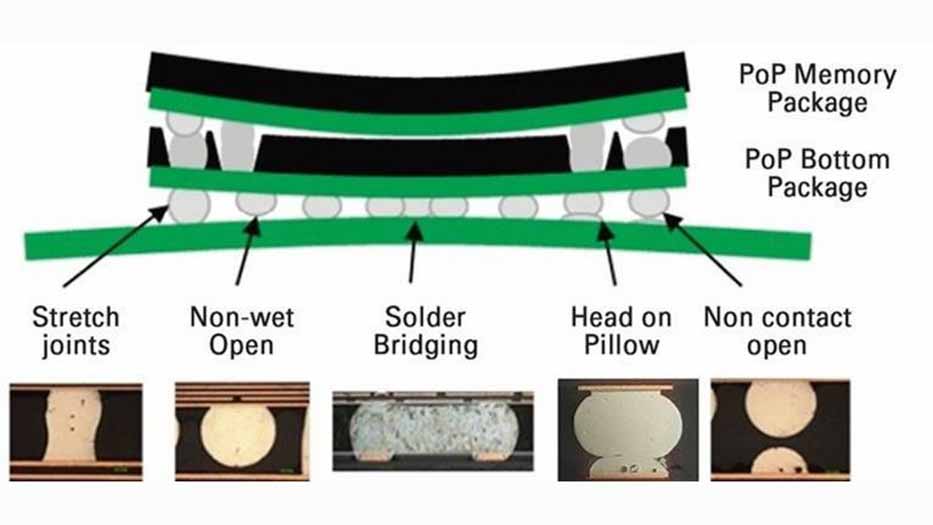
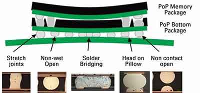
- Failures such as open solder joints and/or shorts of solder joints.
- PCB Assembly Warpage at the fabrication level causes solder printing (soldering defects) issues due to its non-planar nature geometry.
- Alignment issues when mounted using pick and place and even damages the equipment’s nozzle or PCB itself.
- Causes the components to shift/tilt from the initial position while undergoing Re-flow soldering process.
- Warped PCBA’s might not fit in an enclosure & will become a scrap.
Prevention & Solutions
Effective measures to be taken During Design and Fabrication stage.
- Maintaining a correct copper weight and copper etched percentage balance between dielectric layers and copper layers in PCB center.
- Symmetrical circuit board stacking.
- Increase the thickness of the board
- Reduce the size of the board and the number of panel
- Use Router instead of V-Cut Process.
Effective measures to be taken During Assembly Stage.
- Storing PCBs properly in a temperature & humidity-controlled environment before initiating assembly Process.
- Heat processing (heavy-pressing of the PCB’s between heated smooth steel plates for 3 to 6 hours.
- Baking the PCB’s as per recommended Baking Profile.
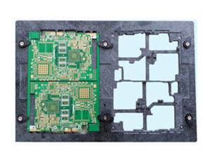
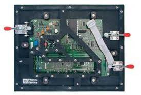
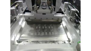
- Use SMT Carrier template/Pallet :- SMT pallet design along with process control will help alleviate the issues that occur due to PCB warpage and will provide margin back to the board assembly process.
- SMT Pallet can be used to support the PCB’s while Solder Paste Printing, Pick and Place and Reflow soldering. It gives the board support around its entire edge.
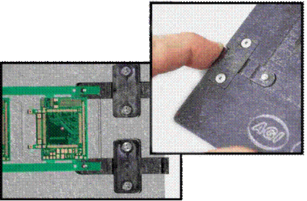

SMT Reflow Carrier Pallets
- PCB supported with carrier pallet can be set to the solder paste printer conveyor/ base plate thus to get a uniform alignment for enhancing the printing quality. This would result in avoiding soldering defects due to disturbed paste.
- Like above, the support pins in the SMT carrier plate/Pallet will help the PCB ot maintain a planar geometry & thus it provides uniform clearance height all over the PCB. This allows the P&P machine to pick and Place the components properly without an error.
- While re-flow soldering, this SMT re-flow pallet facilitates a controlled expansion & contraction and when the temperature of the PCBA comes lower than the Tg value, it maintain the original size by starting to harden again. This supports the edges of the board and prevent bowing across the board width at the time of forced cooling process
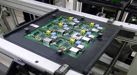
PCB’s from the SMT P&P to the Re-flow Oven
Pallet Design Guideline
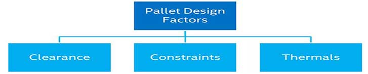
- Clearance:- It’s required to compensate for PCB & Pallet thermal expansion. The Board and the pallet will expand at different rates during reflow due to a difference in their thermal mass and a clearance is needed between the PCB and the pallet to prevent interference during SMT reflow.
- Constraints:- Minimizing constraints in reflow pallet design allows the PCB to expand freely which in turn helps to minimize PCB warpage in the reflow process.
- Thermals:- Maintaining a thermal equilibrium between the pallet and PCB plays a significant role in minimizing the PCB warpage.
EMSxchange Enables you to select a Printed Circuit Board assembly suppliers meeting your Required PCBA Manufacturing Capability, capacity and Certification Criteria from a global PCB Assembly manufacturer base. EMSXchange takes complete responsibility and ownership for your electronic manufacturing process and all its deliverables from contract manufacturing supplier selection to manufacturing to quality inspection to shipment and delivery to your door. EMSxchange Electronic Manufacturing Partners Profile includes:
Argus Sytems (AESPL) – PCBA, Cable Assembly, Box Build.
Cerra Systems inc – PCB Manufacturing.