PCB Testing Types
PCB testing is undoubtedly the most significant step in the PCB manufacturing process because of how crucial printed circuit boards are to our daily lives and how necessary it is that they perform as designed. There is no way to know for sure that a printed circuit board will function properly until tests are carried out to confirm that it operates as expected.
Understanding a PCB manufacturer’s inspection and testing skills is crucial before thinking about partnering with them. Learn more about some of the most popular PCB testing process now in use and why testing is regarded as the most crucial stage of the manufacturing process.
Solderability Testing
Assembly-related problems may originate mostly from the PCB manufacturing process. Many manufacturers test component and PCB pad in order to reduce the possibility of failure. The process of increasing the probability of producing a solid solder joint and minimizing failure is known as solderability. It also ensures the surface’s robustness.
By reproducing the solder’s contact with the material, the solderability failure method measures a solder’s strength and wetting ability. The components’ ability to be assembled can be confirmed by conducting a solderability test.
Many different applications can benefit from solderability testing, including:
- PCB coating evaluation
- Solder evaluation
- Flux evaluation
- Benchmarking
- Quality control
PCB Contamination Testing
Contamination can result in problems including the quick deterioration of wire bond interconnects, including corrosion, degradation, and metallization. One of the most common reason of part failure is contaminations.
During the manufacturing of PCBs, a lot of manufacturers use aggressive chemical process, such as the following:
- Copper etching liquid
- Hot air levelling fluxes
- Electrolytic solutions
- Water-soluble soldering
Chemicals are needed during the cleaning process to ensure proper cleaning. Contamination testing developed by the electronic industry can aid in determining the cleaning procedure’ stability and effectiveness.
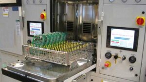
The level of ionic contamination present in a sample is determined via contamination testing. The PCB sample is immersed into solution during the contamination test. Ionic pollution enters the solution once it has been dissolved, changing the composition of the solution and significantly affecting the results or readings.
The analyst maps the contamination level on a contamination test after the results are in, and they are then compared to industry standards.
When the reading goes above a pre-determined level, it is confirmed that the manufacturer’s cleaning procedure is incorrect. When the contaminations are still in the PCB, it can have negative impacts like corrosion and electro-chemical migration. Even the smallest contamination can be detected using this method.
Optical Microscopy or Scanning Electron Microscopes (SEM)
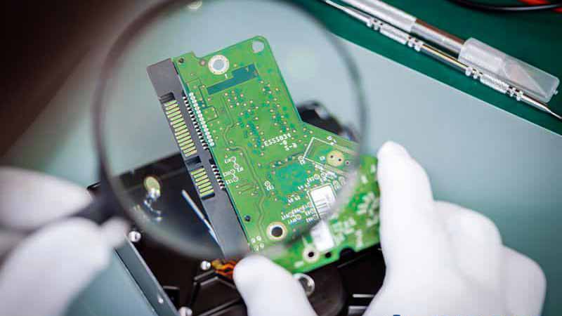
One of the most popular and effective testing methods for detecting PCB faults and failures related to soldering and assembly is optical microscopy. The best optical microscope for locating PCB faults is both quick and accurate.
The optical microscope has a limited depth of field, a single plane of features to be seen, and a magnifying power of up to 1000X.
More powerful magnification tools are often needed for PCB failure analysis in order to find the problem in the PCB.
SEM provides incredibly efficient testing methods for analysing semiconductor die failures. SEM Microscopes can magnify objects up to 100,000 times and provide detailed images. Magnifications of 50,000 to 100,000 and feature resolutions as low as 25 angstroms are usual. For the analyst, this is one of the greatest ways to identify the faults in the images.
A three-dimensional image of the sample and thorough failure analysis are both provided by SEM technology. Also, it may confirm the quality, integrity, and metallization of semiconductor dies. SEM also detects the metal used and offers proof of heat treatment.
X-ray Inspection
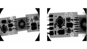
With the use of X-ray inspection, users can apply the tools to find actual or potential defects. They can also use these techniques to inspect a part that has under-the-chip joints or other hidden parts. Instead of using tools with visible light, the analyst might examine the PCB using X-ray inspection.
The analyst is able to do the following internal component inspections with the aid of X-ray inspection capabilities.
- Internal Particles
- Internal wire dress
- Die attach quality
- Voids in the sealing lid
- Substrate/printing wiring board trace integrity
- Insufficient Excessive or Poor solder
By preserving materials in their pre-testing form, this X-ray inspection testing method has the capacity to discover surface and internal faults without causing damage.
EMSxchange Enables you to select a Printed Circuit Board assembly, cable & wire harness assembly and box build suppliers meeting your Required PCBA Manufacturing Capability, capacity and Certification Criteria from a global PCB Assembly manufacturer base. EMSXchange takes complete responsibility and ownership for your electronic manufacturing process and all its deliverables from contract manufacturing supplier selection to manufacturing to quality inspection to shipment and delivery to your door. EMSxchange Electronic Manufacturing Partners Profile includes:
Argus Sytems (AESPL) – PCBA, Cable Assembly, Box Build.
Cerra Systems inc – PCB Manufacturing.


