You are currently viewing 
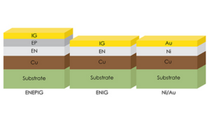
Electroless and Electrolytic Plating of PCB

Electroless Nickel and Immersion Gold Metallization

Electroless Nickel / Immersion Gold is a metallization finish used for printed circuit boards with fine-pitch and finer (<=25 mil) surface mount technology (SMT) and ball grid array (BGA) designs.

Electroless Nickel metallization occurs after copper trace/feature definition (i.e. after Cu plate, image and etch operations). It can be applied before or after the solder mask application. It thus provides a conformal coating on all exposed copper surfaces (i.e. on all trace and feature tops and sidewalls).

It uses a multi-step process (using a palladium catalyst) in chemical processing tanks to chemically deposit a nominal 150 – 200 micro-inches of approximately 92% purity nickel over exposed copper traces and features. Intrinsic to the electroless process is a significant amount of phosphorous (˜ 8 to 11%) that is co-deposited with the nickel, which reduces the nickel ductility to &lt;1% elongation (i.e. it becomes much more brittle than pure nickel).

The nickel acts as a barrier layer between the copper and the gold, preventing unwanted (unsolder able) intermetallic formation. The nickel layer also adds strength to plated through holes and vias. The inherent hardness of nickel effectively increases wear resistance.

Immersion Gold occurs after the electroless nickel process (and thus after copper image definition). It also provides a conformal coating on all exposed nickel surfaces (i.e. on all trace and feature tops and sidewalls).

It is a molecular replacement process in which previously deposited nickel molecules are replaced by gold molecules in a chemical processing tank. The gold deposited is ˜99.99% pure, and its thickness is allowed to build up to 3 to 8 micro-inches. Although immersion gold is a somewhat porous conformal final metallization, it does provide excellent corrosion resistance and solder ability properties, and it retards the passivation (oxidation) of the nickel layer.

The combined nickel/gold metallization provides excellent corrosion resistance, solder ability, pad planarity, and shelf life. It is a good choice for fine-pitch and finer (<=25 mil) SMT and BGA technologies.

Electrolytic Nickel and Gold Metallization

Electrolytic Nickel / Gold is a standard metallization finish used for through-hole, SMT, and BGA assembly technologies.

Historically, it has been used for through-hole boards, but improved capabilities have given it new life in use for standard- to extra fine-pitch (50 to 20 mil) SMT and BGA technologies. Some customers use electrolytic Ni/Au as their standard metallization for their high density, 5/5 mil trace, and space SMT and BGA printed circuit board designs (e.g. computer, workstation, and medical products).

Electrolytic Nickel occurs after copper image definition (i.e. after Cu plate and image operations) but before etch and solder mask application. Thus it provides a coating only on the top surfaces of all exposed copper traces and features.

Electrolytic nickel metallization is affected by electrically driving nickel ions to bond with exposed, electrically connected copper traces and features in chemical processing tanks.

Nickel is plated on the exposed copper traces and features to a nominal thickness of 200 micro-inches for standard production 5/5 mil trace and space geometries. For finer trace and space geometries (4/4 mil), the nickel plated can be reduced to a nominal thickness of 175 micro-inches.

Electrolytic nickel acts as a barrier layer to Au/Cu intermetallic adds strength to plated through-holes and vias and increases wear resistance.

Electrolytic Gold metallization occurs after electrolytic nickel, and thus after copper plate and image operations but before etch and solder mask application. The gold also provides a coating only on the top surfaces of all exposed nickel traces and features. Thus, after final etch operations, there is a small area of trace and feature sidewalls (i.e. Cu and Ni) that are exposed.

Electrolytic gold, also known as flash gold is plated to a nominal thickness of 3 to 10 micro-inches, and it too builds up only on the tops of exposed traces It has excellent corrosion resistance and solder ability properties (as well as sealing the nickel surface to eliminate passivation).

This combined nickel/gold metallization provides very good corrosion resistance, good to excellent solder ability, pad planarity, and shelf life. It is a good choice for standard- to extra fine-pitch (i.e. 50 to 20 mil) SMT or BGA technology.

Thin electrolytic gold (i.e. 3 – 10 micro-inch) is not typically used for wire bonding technology and PCB manufacture provides thicker electrolytic gold (30 micro-inches) which is suitable for wire bonding.

Comparison of ENIG Metallization and Electrolytic Nickel and Gold Metallization

For the parameters of corrosion resistance, shelf life, nominal metal thickness, metal purity, and solder ability, both electroless Ni/immersion Au and electrolytic Ni/Au provide good to excellent performance.

Either metallization would be a good choice for standard- through extra-fine pitch (i.e. 50 to 20 mil) SMT or BGA technologies. For ultra-fine pitch and less (<=16 mil pitch), only the electroless Ni/immersion Au process has been tested. For PCB designs using 4/4 mil minimum trace and space, either metallization has the capability and will provide acceptable performance.


EMSxchange
 Enables you to select a Printed Circuit Board, PCB Assembly, cable & wire harness assembly, and box-build suppliers meeting your Required Electronic Manufacturing Capability, capacity, and Certification Criteria from a global Electronic contact manufacturer base.

EMSxchange takes complete responsibility and ownership for your electronic manufacturing process and all its deliverables from contract manufacturing supplier selection to manufacturing to quality inspection to shipment and delivery to your door.

EMSxchange Electronic Manufacturing Partners Profile includes:

Argus Systems (AESPL) – PCBPCBACable AssemblyBox BuildTesting.

Aura – Electronics system design Services & consulting