X-ray Inspection in Electronic Manufacturing
X-ray inspection technology, often known as automatic X-ray inspection, is a type of X-ray inspection (AXI). These are unique rays with incredibly short wavelengths and intense electromagnetic waves. The wavelength is less than 10 nano meters, which is much shorter than visible light. The great penetrating power of x-ray makes it suitable for use in industrial settings. An X-ray can see through a substance that is invisible to the naked eye. X-ray inspection is now widely employed in a variety of industries, including medicine, industrial control, and aerospace. Throughout terms of PCB inspection, X-rays are widely employed in the PCB assembly process to evaluate the PCB’s quality, which is one of the most critical processes for a quality-conscious PCB maker.
Typical PCBA x-ray inspection system supports 2.5D X-ray imaging service, i.e. 2D X-ray images with an oblique view of 70 degree, There are also PCBA inspection based on CT technique which captures several 2D x-ray images from different angles and then uses reconstruction algorithms to create the 3D model for advanced mode detailing. The traditional X-inspection system has many shortcomings such as long time X-ray exposure, high working voltage, strong radiation, critical environmental requirements, especially very costly.
Now a days X-ray inspection system, using a semiconductor scintillated image sensor plate and X-ray tube generator, provides extreme short exposure time(only 0.4-4 seconds), remote control operation, small size, less radiation, clear image at affordable prices.
Typical specification of 2D x-ray inspection system:
- Resolution 20um.
- X-Ray Tube Generator 70eKV, 3ma, focal spot 300um, closed mode.
- Fixed anode, max power: 150 Watts.
- X-Ray Leakage/Exposure Time <1μSv/h, 0.4-4.0 second time setting by a Touch panel X-ray exposure timer.
- X-Ray Controller Mode Remote control(30-50 meter)
- Flat Image Sensor Resolution 2.1Mpixel, 22lp/mm, 20um/pixel size.
- Active Image Area and Format 30*30mm, JPG,BMP,TIF, DICM,RAW.
- Image magnification(by software) 20x-50x.
- Fixed work station(with LED light) , 200*200cm platform.
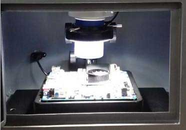
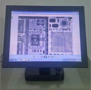
How X-Ray Inspection Works?
To comprehend what x-ray PCB inspection entails, you must first comprehend how x-ray inspection operates. All x-ray inspection devices have three basic characteristics:
- X-ray tube: This tube is capable of producing x-ray photons.
- Platform: The operating platform allows the sample to be inspected from multiple angles and magnitudes by moving it in different directions.
- Detector: On the other side of the sample, the detector captures and gathers x-ray photons before converting them to a picture.
X-ray imaging uses photons of x-rays that travel through a material and are captured on the opposite side. The physical qualities of materials, such as atomic weight, density, and thickness, affect how x-ray photons flow through them.
Heavy elements absorb more x-ray photons and are thus easier to photograph, whereas lighter elements are more transparent. Because various materials act differently, photons collect in varying amounts on the other side of the object, resulting in a picture. A PCB’s components are often made up of heavier elements, making them visible on an x-ray image.
Case studies of PCB Assembly Xray Inspection
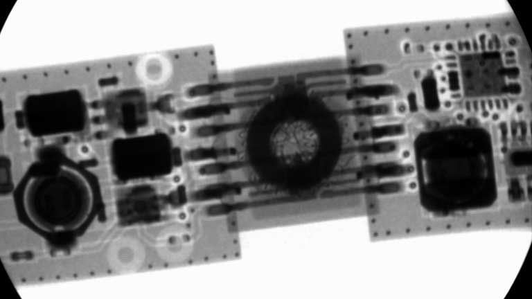
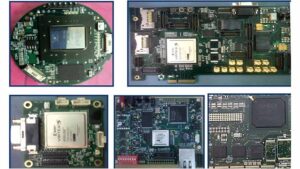
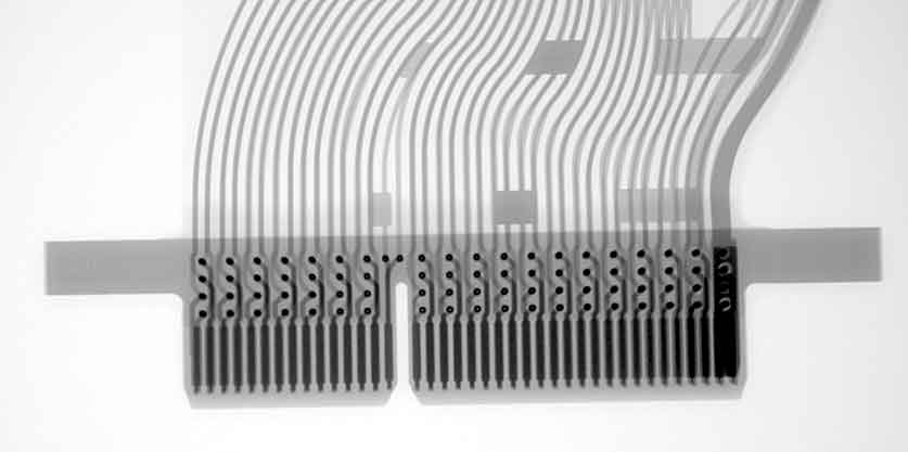
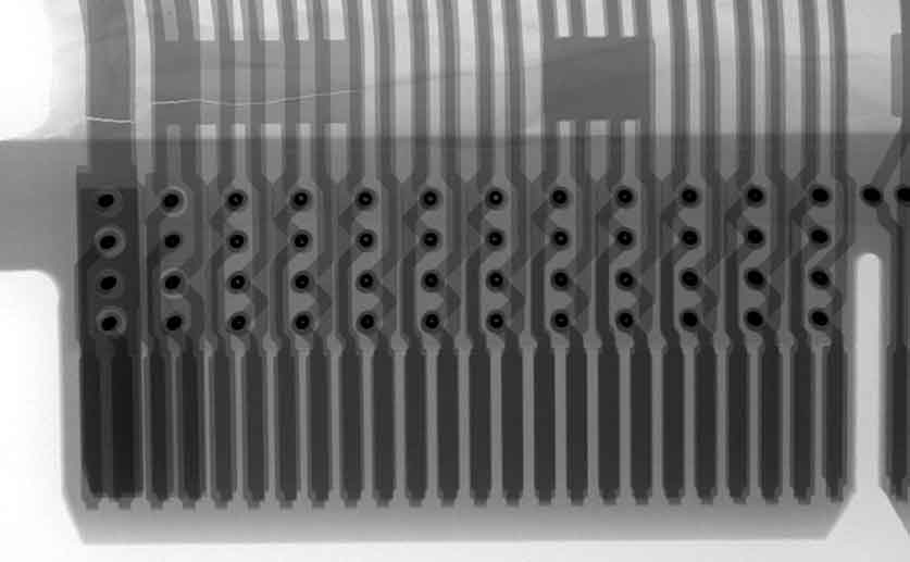
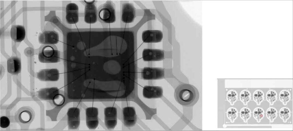
Materials absorb X-rays proportionally to their atomic weight, and all materials absorb X-ray radiation differently depending on their density, atomic number, and thickness. Heavy-element materials absorb more X-rays and are easier to image, whereas lighter-element materials are more transparent to X-rays. Have a look on some examples given below.
PCBA- Xray
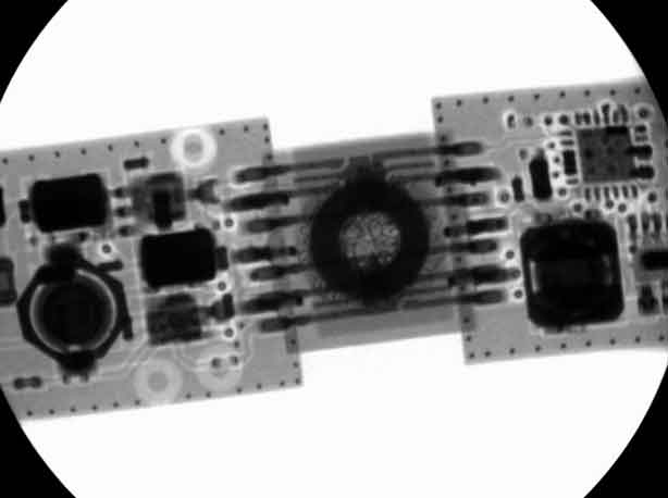
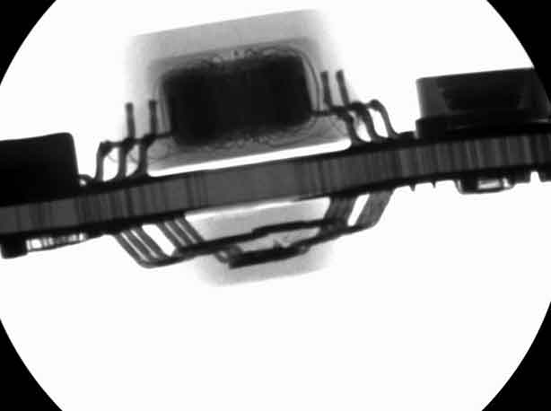
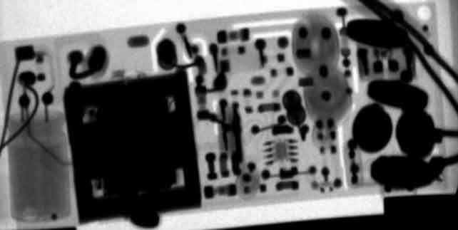
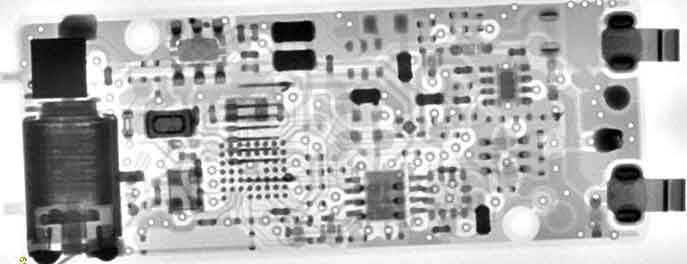
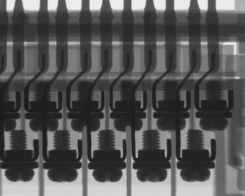
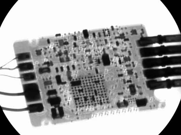
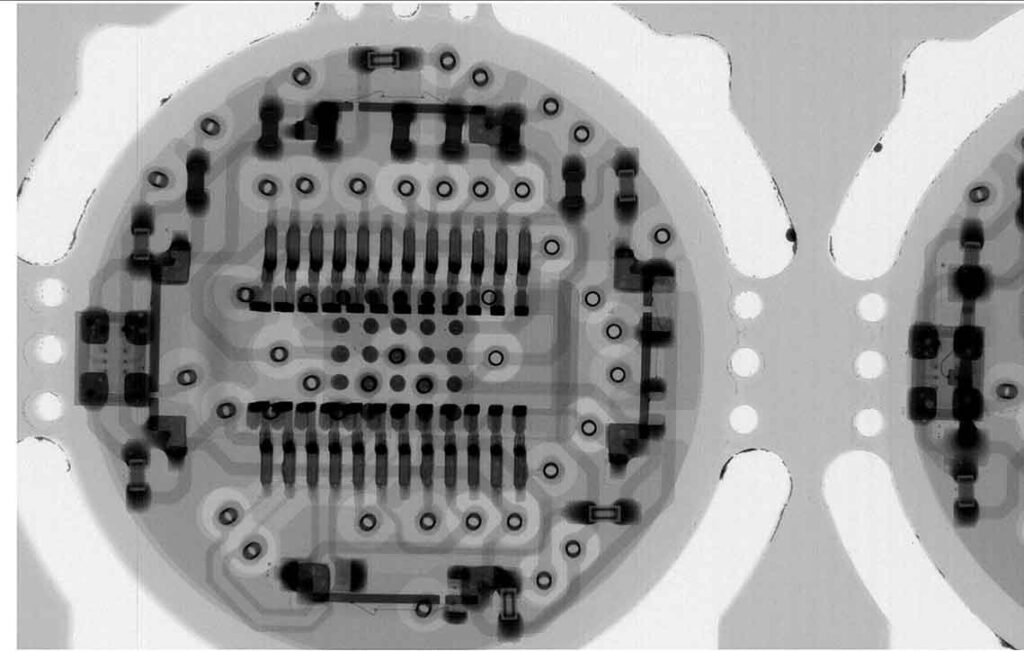
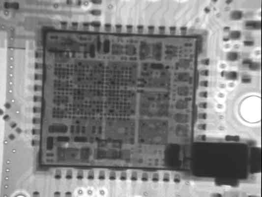
BGA Xray
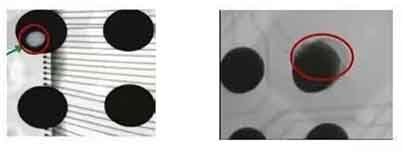
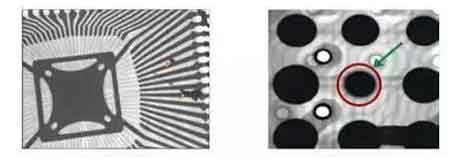
Cable assembly Xray
QFN Xray
Why X-Ray Machines Are Becoming Popular?
Over the last several decades, electronics manufacturing has become increasingly sophisticated, with electronics in the industrial, communication, military, and aerospace industries progressing in ways that make inspection much more challenging. The following are some of the most prominent trends that have a detrimental impact on inspection:
- Component placement: To reduce space and maximise functionality, equipment is becoming smaller and more stacked. As a result, many solder joints and components in electronics are being shifted to interior layers, either between PCB layers or hidden within the finished device.
- Component size: Miniaturization of circuit board components is becoming more prevalent. PCB components are projected to follow this trend as the requirement for more dense boards grows.
- SMT: Surface mount technology reduces the size of leads and packages, resulting in higher density PCBs with more components buried between layers.
Traditional inspection methods have become practically impossible to discover flaws thoroughly because to the increasing density, decreasing size, and more complex positioning of PCBs and their components. Due to the density of current PCBs, optical, ultrasonic, and thermal imaging methods are inadequate.
X-ray inspection, on the other hand, can acquire detailed images that these other technologies cannot. Because X-ray can penetrate PCB layers to inspect interior layers and packaging, it is more suitable for inspecting solder joints on complicated PCB assemblies. As a result, PCB examination using x-ray technology is becoming more common.
EMSxchange Enables you to select a Printed Circuit Board assembly, cable & wire harness assembly and box build suppliers meeting your Required PCBA Manufacturing Capability, capacity and Certification Criteria from a global PCB Assembly manufacturer base. EMSXchange takes complete responsibility and ownership for your electronic manufacturing process and all its deliverables from contract manufacturing supplier selection to manufacturing to quality inspection to shipment and delivery to your door. EMSxchange Electronic Manufacturing Partners Profile includes:
Argus Sytems (AESPL) – PCBA, Cable Assembly, Box Build.
Cerra Systems inc – PCB Manufacturing.

