Flying probe testing of PCBs
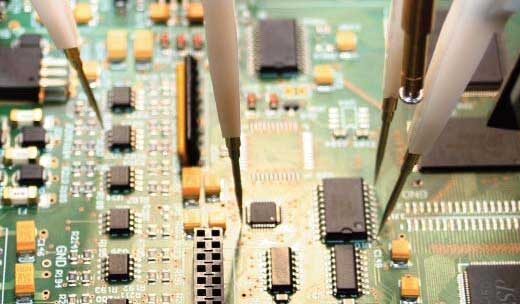
Flying probe testing uses “flying” test probes that move from one test point to the next in accordance with the instructions provided by the individual software programme designed for the board under test. If utilised on an assembled PCB, it might alternatively be referred to as a fixtureless in-circuit test ( ICT ) because no custom fixture is required. As a result, it’s ideal for prototypes and low- to mid-volume production.
Flying probe testers were developed specifically for bare board testing and have since become the standard for bare-boards testing as well for PCB assemblies in which the major electrical characteristic assessed is the resistance between two points or nodes. flying probe testing is commonly used for test of analog & Digital components, analog signature analysis and short/open circuits.
Early flying probe testers Could only test passive components or diodes however to accomplish higher levels of fault detection, boundary scan and the utilisation of on-board memory are used. This allows for more complex tests to be performed. To verify that the individual flying probe tester can meet the requirements, it is required to check its performance.
Advantages of a flying probe test system:
- No special fixture required and Eliminates fixture making cost and time:
The “bed of nails” apparatus necessary for ICT is not required because the probes move according to software control to make contact with the required nodes. To keep the board in place, a basic generic mechanism is required.
- Changes can be made easily:
Any modifications to pad placements or components can be done by simply altering the programme because the probes move under software control. As opposed to a “bed of nails” fixture, no mechanical adjustments to a fixture are required. Since it has controlled probe contact, it can be programmed for any type of board.
- Reduced test development time:
The PCB design files can be used to quickly construct software for a flying probe tester. There is a significant cost savings because no mechanical fixture is required, and no manufacturing time is required. As a result, all that is required to construct the test programme for the flying probe tester are the PCB files and, eventually, a first-off board or boards on which to test the programme. In summary it allows for Quick test program development, easy integration of design changes and process flexibility.
- Integrated Test solutions:
Its is feasible to Integrate Different test solutions and approaches to Flying probe testin environment. For example most of FPT systems offer a Combination of the flying probe, boundary-scan and functional test environment.
Also many of the Flying probe test systems supports Visual tests for component presence/absence and rotation with Automatic Optical Inspection (AOI) and fixed electro scan capabilities.
Challenges of a flying probe test system:
- Speed of operation is slow:
The flying probe tester is substantially slower than other types of automated test equipment, such as an ICT, because the probes must physically move to each location in turn. All of the connections for an ICT system are already in place in the fixture.
- It may not always possible to make complicated tests.
The advantages of the flying probe test system make it perfect for a wide range of applications. With the present trend of miniaturising electronics, flying probe tests are becoming increasingly popular. Smaller devices have smaller circuit boards, making FPT testing more cost-effective. A flying probe tester also makes programming complex and dense boards easier.
By balancing the advantages and disadvantages of the flying probe test system, it is well suited to prototype applications as well as sectors where small-scale manufacturing is carried out. It is not suited for volume production applications due to the test times unless it is just used for sample testing due to the test timeframes.
How does Flying Probe Testing work?
A flying probe test is simple to use. The steps are as follows:
Step 1:
The first step is to write an FPT test programme to verify the circuit board assembly. The test programme is usually created on an offline PC with the help of an FPT test programme generator application. The Gerbers, BOM, and ECAD files for the PCB assembly are required by the programme. The ECAD file should be an intelligent CAD file, and the BOM should be in EXCEL format.
Step 2:
The next step is to load the test programme onto the FPT tester when it has been created. A conveyor belt inside the tester transports the circuit board assembly that needs to be tested. A single circuit board or a series of circuit boards can be used. The board will be transported by conveyor belt to the area where the investigation will be conducted. The probes’ contact with the pads and exposed vias is controlled by the test programme.
Step 3:
Following that, the FPT applies power and electrical test signals to the probe locations before reading the results. If the measurement readings are processed further, it will be determined if a specific circuit piece fulfils the predicted findings. Any divergence from established programmes and expectations will indicate a unit flaw, resulting in a failed test.
Flying probe Testing Guidelines
To limit the issue of board damage and improve test accuracy during a flying probe test, follow the guidelines and recommendations below.
Cleaning:
Before testing, make sure the probe regions and the assembly are clean. This can be accomplished by eliminating all flux or ensuring that pin probe-able flux is used during manufacture. Cleaning the assembly ensures quick contact, reduced testing time, and consistent results. Cleaning the assembly can result in a false fail, and if the tester has to shift its location repeatedly to guarantee better contact, test duration can increase.
Board Rail:
A 3 mm wide border edge free of any component shall run along the opposing sides of the PCB. This blank space will be used to handle the PCB within the machine. Space in the board’s design or panel waste can make up the border edge.
Fiducials:
To properly position the probes on testing equipment, fiducial markers or reference points are required. These points are normally found on the panel waste, but they can also be found on the printed circuit board, which is useful if the panel waste isn’t there.
Component Legs:
On the “toe,” there should be enough room to probe near the component legs. As a result, a good solder joint will be possible. During tests, however, it is better not to probe the component legs directly, as the probe pressure can force the component legs onto the pad, causing any potential open circuits to be corrected.
Vias:
It is feasible to probe the edges of PCB vias. Exposing the vias rather than concealing or tenting them, on the other hand, is likely to yield better outcomes. The “non-tented” criteria should be included in the PCB design.
Probe Points:
For the ground and power rails, it is recommended that probe points be located on the bottom side of the PCB. Easy-to-reach probe sites can cut test time in half and lower total costs.
Height of the component:
The heights on both sides of the PCB should be kept to roughly 40 mm and 90 mm, respectively. When that height is exceeded, a “No Fly” zone is created, making access to the assembly difficult.
Accessibility Check:
On single-sided machines, it’s desirable to allocate at least one side of the assembly for testing, as this reduces the cost of turning the board over and testing both sides.
Size:
Flying probe tests are time-consuming because they need moving probes between measurement places, which takes time. Keep access points close together to reduce this time, especially on a big PCB.
Features of Typical Flying probe tester
- 5 mobile electrical probes, 1 mobile open fix probe.
- 8 fixed probes.
- 2 CCD camera.
- Intrinsic Positioning and measurement precision.
- Vector-less tests (JSCAN and OPENFIX) to test ICs for opens and shorts.
- FNODE signature analysis on the nets of the UUT.
- PWMON net analysis for power on the boards.
EMSxchange Enables you to select a Printed Circuit Board assembly suppliers meeting your Required PCBA Manufacturing Capability, capacity and Certification Criteria from a global PCB Assembly manufacturer base. EMSXchange takes complete responsibility and ownership for your electronic manufacturing process and all its deliverables from contract manufacturing supplier selection to manufacturing to quality inspection to shipment and delivery to your door. EMSxchange Electronic Manufacturing Partners Profile includes:
Argus Sytems (AESPL) – PCBA, Cable Assembly, Box Build.
Cerra Systems inc – PCB Manufacturing.


