
PCB Depanelization
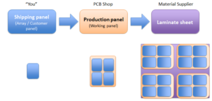
PCB panelization is a manufacturing technique in which smaller boards are manufactured and connected together in array form, making it easier to move through an assembly line. The individual boards can easily be depanelized or removed from the array for packaging or installation into a product.
The de-paneling is the separation of pcb from the panel and it will take place at some point in the production process, such as after the circuits have been tested or after all the components have been mounted on the board.
There are many ways to depanelize the boards. It depends on how you chose to connect the boards to each other in the panel.
V grove method:
Also known as v-scoring, this method involves tracing a V-shaped cut along the top and bottom edge of the panel. Typically, boards are scored to about ⅓ the thickness. A fixture or machine must be used to depanel it, as manual removal can put undue strain on components towards the edge.
Mouse bites method:
Mouse bites in PCBs refer to little perforations on boards. In addition, mouse bites look like half holes on a postage stamp. So, these perforations allow small boards to connect in a group.
PCB De-paneling Methods
PCBs can also be built as single pieces if necessary, however they are commonly produced as big panels with several boards at once. Depanelization of PCBs can be done manually, fully automatically, or semi-automatically. The electronics industry uses a number of methods, including laser PCB depaneling, Here are some of the PCB Depaneling methods that you must know about.
Punching/Die Cutting:
The punching method involves using a special fixture to punch individual PCBs from the panel. Sharp blades and supports are located on opposite sides of the punching device. Each board needs a distinct die, and in order to keep them sharp, dies must be often changed. Despite the high production rate, the specially made fixtures and blades have ongoing costs.
V-Scoring:
To minimise overall board thickness, boards are scored along the cut line on both sides. Then the PCBs are removed from the panel. A depth of around 30% of the board’s thickness is sliced into the panel on both sides. Boards can be manually removed from the panel once they have been filled with data. The boards are under stress, which may break some of the components or the solder connections, especially those that are close to the board’s edge.
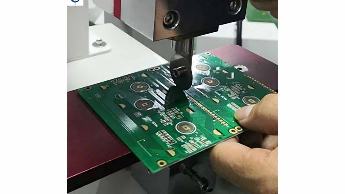
Wheel Cutting/Pizza Cutter:
The “pizza cutter” technique is a manual substitute for breaking the leftover web after V-scoring. As the V-score and cutter wheels must be precisely matched, accuracy is essential. On board, there is a little amount of stress that can harm some components.
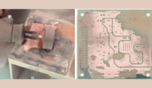
Laser Depaneling
Boards requiring high tolerances can be depaneled using a laser. Through a computer-controlled process, depaneling takes place without any physical contact, without any mechanical stress, and is customizable to cut requirements. Laser depaneling can be used in surface mount technology (SMT) lines or used independently with board unloaders and loaders.
Routing:
The majority of PCBs include narrow tabs connecting each circuit to the panel frame, which are then broken or snapped to separate the circuits. Due to the huge kerf width of a physical bit, routing can consume a significant amount of panel space.
Laser Routing:
Without the use of any mechanical dies or blades, laser routing offers an entire software-controlled procedure. Any path, including ones with bends and sharp corners, can be sliced with laser routing. With remarkable accuracy, the cut kerf width can be less than 20 microns.
Laser routing can be performed using either:
High-power CO2 laser (~10µm wavelength)
FR4, glass fibres, and other rigid and flex circuit substrates can all be thermally cut by a CO2 laser at quite high speeds, however most substrates will experience a notable heat impact along the cut edge.
Solid-state UV laser (355nm wavelength)
The UV laser ablates the panel material with far less heat and a smaller kerf width thanks to its significantly smaller focused spot size. However, due to lower power levels, UV lasers have slower cutting speeds than CO2 lasers and cost more per watt than CO2 lasers.
Users who clean the circuits after singulation can profit from the increased speed of the CO2 laser, whereas companies that are sensitive to char and small debris along the cut line would typically use the UV laser.
EMSxchange Enables you to select a Printed Circuit Board assembly, cable & wire harness assembly and box build suppliers meeting your Required PCBA Manufacturing Capability, capacity and Certification Criteria from a global PCB Assembly manufacturer base. EMSXchange takes complete responsibility and ownership for your electronic manufacturing process and all its deliverables from contract manufacturing supplier selection to manufacturing to quality inspection to shipment and delivery to your door. EMSxchange Electronic Manufacturing Partners Profile includes:
Argus Sytems (AESPL) – PCBA, Cable Assembly, Box Build.
Cerra Systems inc – PCB Manufacturing.